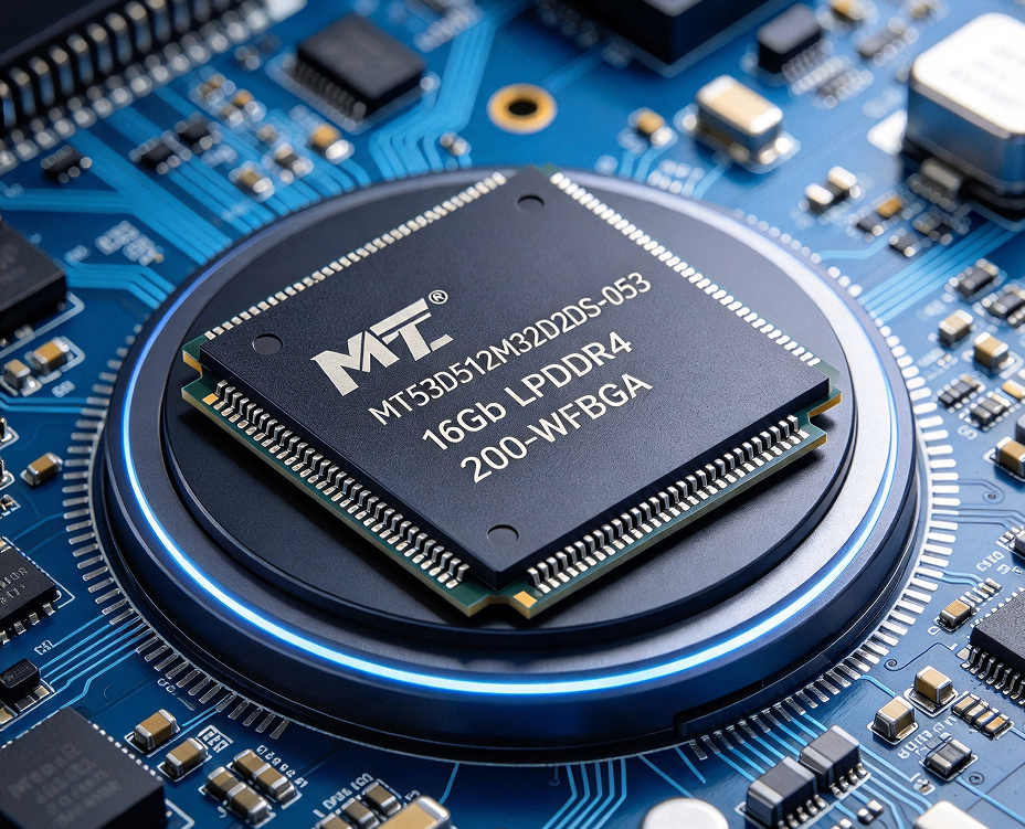
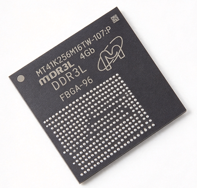
NT5TU32M16FG-AC Complete Data Sheet, Specifications and Pinout Guide
ThisNT5TU32M16FG-ACPresented here in a single-page format, specifically designed for engineers, this document extracts key data sheet information to accelerate DDR2 subsystem design. This brief overview highlights memory density levels, nominal voltage ranges, and typical data rate ranges, while emphasizing that final verification must still refer to the official data sheet. This guide focuses on core points: critical specifications, pinout diagrams, timing characteristics, PCB/layout recommendations, and a practical design checklist.
1 — Quick Overview and Key Data Sheet Points (Background)

What is NT5TU32M16FG-AC?
Key points: This device is a DDR2 SDRAM with a 32M×16 organization and a storage capacity of 512 Mbit, designed to serve as a memory component in embedded systems and modules. Basis: The manufacturer's datasheet lists the device's organization, nominal Vcc/Vddq supply voltage range, and supported speed grades; designers should refer to this information for parameter values specific to each model. Note: Treat this device as a single-sided, 16-bit-wide DDR2 memory chip suitable for systems with moderate requirements for memory density and DDR2 timing characteristics.
Key Specifications at a Glance (Datasheet Snapshot)
Key points: A concise specification summary clearly identifies the parameters that designers should check first: density, organization, data rate range, supply voltage, package type, and temperature grade. Basis: The datasheet explicitly states the organization (32M x 16 = 512Mbit), a nominal Vcc/Vddq of approximately 1.8V, DDR2-level data rates, and a BGA package with multiple speed/package variants. Note: Please use the table below as a quick reference, and verify the speed grade, ball count, and current values in the official datasheet before layout or procurement.
| Parameter | Typical Value/Note |
|---|---|
| Density/Organization | 512 Mbit (32M x 16) |
| Data Rate/Clock | DDR2 level (refer to the datasheet for specific speed grades) |
| Supply Voltage | Vcc / Vddq ≈ 1.8 V (nominal) |
| Package | BGA package variant (please verify ball count and pad layout) |
| Temperature Grade | Commercial/Industrial-grade variants (see datasheet for details) |
| I/O Standard | SSTL_2 / DDR2 Signal Transmission |
2 — Electrical Characteristics and Absolute Maximum Ratings (Data Analysis)
Power Supply, Current, and Power Consumption Ranges
Key Points: Power rails and current consumption determine the power sequencing and thermal budget of the design. Basis: The datasheet provides minimum/typical/maximum voltage values for Vcc/Vddq, current ranges during operation and standby, as well as clear power-up sequencing rules that must be followed. Explanation: Measure current at device-level power pin reference points, evaluate IR drop on the PCB, and ensure decoupling and plane design meet the peak operating current and surge current requirements specified in the datasheet.
Timing Window Affecting Performance
Key points: Timing parameters such as tCK, CAS latency, and cycle time determine the achievable throughput. Evidence: Critical timing specifications (tCK, tCL, tRCD, tRP, tRAS, burst length) are listed in the datasheet by speed grade to define the controller's timing budget. Explanation: Use these values to calculate the maximum theoretical bandwidth, configure the controller's timing margins, and verify through simulation and chip debugging that the design meets the requirements.
3 — Pinout and Package Mapping (Methodology Guide)
Package variants and ball/lead mapping
Key point: Accurate package and ball grid mapping can prevent footprint and routing errors. Evidence: The datasheet provides mechanical drawings, BGA ball grid maps, and recommended pad layouts for each package variant and speed grade. Explanation: Reproduce or reference the ball grid map from the datasheet in your PCB design tool, and before generating manufacturing data, verify the specific number of balls and mechanical dimensions for each variant against the bill of materials.
Signal groups and functional pin groupings
Key points: Grouping pins by functional modules can simplify floorplanning and routing. Basis: The datasheet groups power/ground, address/command, DQ/DQS strobe signals, and NC pins; designers can stack these groupings and use color coding to clearly present the pin arrangement. Explanation: To reduce impedance, power and ground should be placed adjacent to each other; address/command signals should be routed in matched bundles; DQ/DQS differential pairs must maintain strict length matching to ensure timing and signal integrity (this is indicated as a pin arrangement guideline).
4 — Timing Diagrams, Initialization, and Operation Sequences (Data Analysis/Methods)
Considerations related to read/write timing and setup/hold times
Key points: The read/write timing diagram reveals the setup/hold constraints that affect timing margins. Evidence: The datasheet provides waveform diagrams as well as numerical setup/hold parameters for read/write cycles and CAS latency (such as tRCD, tWR). Explanation: Interpret these parameters to configure the controller's read/write window, adjust drive strength and termination to maximize eye diagram opening, and verify during system startup through eye diagram measurements.
Initialization, Refresh, and Power-Up Timing
Key points: Proper initialization and refresh timing are critical for reliable operation. Evidence: The datasheet lists the required sequence of mode register settings, the number of precharge/auto-refresh cycles, and the refresh interval, along with timing constraints and descriptions of fault modes. Explanation: Power up in the prescribed order, set the mode registers, and perform regular refreshes to prevent data corruption; if timing errors occur, record and monitor recurring fault symptoms such as NACK or CRC errors.
5 — PCB Layout, Signal Integrity, and Thermal Management Best Practices (Case Studies/Hands-on Exercises)
Layout Recommendations for DDR2 BGA Package Devices
Key Points: The layout determines the signal integrity performance of the DDR2 channel. Evidence: The best practices guide provides recommendations on fan-out strategies, via escape, power/ground plane stacking, DQS/CK termination, and trace length matching as guiding principles for DDR2 layout. Explanation: BGA pads should use via escapes; the trace lengths of DQ/DQS differential pairs must be strictly controlled within tolerance; decoupling capacitors should be placed close to the Vcc pins; and controlled impedance traces should be used to meet timing and signal integrity requirements.
Thermal Management and Reliability Considerations
Key points: Thermal management and soldering processes affect long-term reliability. Evidence: The datasheet provides recommended reflow soldering profiles and clearly outlines precautions regarding maximum junction temperature and current density. Explanation: Monitor PCB hotspot temperatures, verify solder joint quality according to the recommended reflow profile, and perform IR voltage drop analysis to ensure that the power plane does not fail due to overheating under prolonged operation.
6 — Design Checklist, Debugging, and Verification Techniques (Action Recommendations)
Pre-Silicon and Pre-Layout Checklist
Key points: A comprehensive checklist can reduce late-stage redesigns. Evidence: Items to be verified include pin placement and package selection, power rail timing, timing budget with the controller, decoupling schemes, and simulation modules identified in the datasheet. Explanation: Conduct signal integrity simulations for critical nets, cross-check pad patterns against mechanical drawings, and use the timing windows provided in the datasheet to pre-validate timing convergence before production.
Common Failure Modes and Troubleshooting Steps
Key points: Use symptom-based targeted diagnostics to expedite problem resolution. Evidence: Typical failure modes include startup failures, data corruption, and excessive current; the datasheet helps identify expected signal levels and timing windows for comparison. Explanation: Debug by probing the eye diagram openings of CLK/DQS/DQ, verify power sequencing, and perform isolation tests on decoupling networks; compare oscilloscope-acquired data with the timing and electrical specifications in the datasheet to pinpoint the root cause.
Summary
- This document distills the core contentNT5TU32M16FG-ACThe information provided in the datasheet—including package type, nominal Vcc/Vddq, and key DDR2 timing parameters—can accelerate design decisions without requiring a full datasheet replacement.
- Key design measures: Verify package/ball grid model based on pad layout, ensure proper power-up sequence, and match DQ/DQS trace lengths to guarantee signal integrity and timing convergence.
- Verification Checklist: Perform signal integrity simulations to validate decoupling and power plane design, and during the power-up debugging phase, conduct controlled startup using oscilloscope eye diagrams and timing checks to ensure reliable device integration.
Frequently Asked Questions
For this device, which timing parameters should be prioritized for inspection?
Controller designers should focus on parameters listed in the datasheet, such as tCK, CAS latency (tCL), tRCD, tRP, and tWR. Compare these with the target clock frequency to calculate latency and bandwidth, then verify margins through eye diagram capture and timing simulation during power-up debugging to ensure stable system operation.
Before manufacturing, how can pin assignments and pad layouts be verified?
Please compare the pad layout and ball grid array (BGA) footprint from the datasheet with your CAD package; also, verify the number of balls and mechanical tolerances against the package model, and perform DRC/DFM checks. Before producing the first prototype, quickly review physical samples or stencil templates to identify and avoid mismatch issues.
Which test points can help pinpoint the cause of DDR2 initialization failure?
Check whether the amplitude, timing, and eye diagram opening of the clock (CK), DQS strobe signal, and DQ data lines are correct; confirm that the power rails are powered up in the required sequence, and measure surge current and steady-state current. Compare the captured waveforms with the timing windows specified in the datasheet to detect setup/hold time violations or signal integrity issues.
What is the recommended power-up sequence?NT5TU32M16FG-AC?
Please apply VDDQ before or simultaneously with VDD and VDDL. Ensure that the control signals, address signals, and data signals are in a defined low-level/invalid state. After the power supply has stabilized, apply CK/CK#, initialize the DLL via the Mode Register Set (MRS), and perform the necessary precharge and auto-refresh operations.