NT5CC256M16EP-DI DDR3L 4Gb: Comprehensive Spec Report
The NT5CC256M16EP-DI is presented here as a focused, single-source technical breakdown for engineers assessing a 4Gb, x16 low-voltage DDR3 device. Market and supplier datasheets for similar 4Gb DDR3L devices consistently show a 1.35V nominal supply, x16 organization, and support for high-speed bins up to DDR3-1866; this report synthesizes those common figures into actionable checks and integration guidance.
This article will walk through background context, electrical and timing details, architecture implications, PCB and controller integration rules, typical use-cases and comparisons, and a procurement and lab-validation checklist tailored for embedded and legacy-system design teams.
Background & product context
What "DDR3L 4Gb" means (organization & terminology)
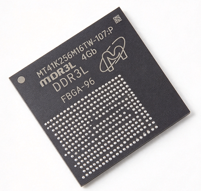
What "DDR3L 4Gb" means is straightforward: 4 gigabits of storage per die arranged in an organization such as 256M x 16, yielding a 16-bit I/O. Industry datasheets classify DDR3L as the low-voltage DDR3 family with a nominal VDD/VDDQ of 1.35V and backward functional compatibility with 1.5V hosts when specified. Engineers should verify exact organization and address mapping before controller integration.
Typical package options & grade variants
Common package types for 4Gb density include small BGA packages with typical ball counts in the mid-double-digits (for example, 96-ball TFBGA variants). Parts are commonly offered in commercial and industrial temperature grades; expected operating ranges span roughly from 0°C to 85°C for commercial and from -40°C to 95°C for industrial variants. Confirm package, ballmap and mechanical dimensions for board-level fit and reflow profiles.
Key electrical and timing specifications (data deep-dive)
Voltage, power & supply tolerances
Nominal VDD/VDDQ for DDR3L parts is 1.35V with typical datasheet tolerance bands near 1.283–1.45V. Datasheets list multiple IDD figures—standby, active, precharge, and burst read/write currents—so designers should extract IDD0/IDD2P/IDD3N values relevant to idle and active modes. For battery-powered and thermally constrained systems, prioritize standby and self-refresh currents as these dominate long-term energy consumption and thermal budgets.
Speed bins, CAS latency & timing parameters
Many 4Gb DDR3L devices support speed bins up to DDR3-1866 (1866 MT/s) with CAS latency variants that commonly span CL9–CL11 depending on speed and binning. Critical timing parameters to collect from the datasheet include tCL, tRCD, tRP, tRAS, tRFC and the command/address timing windows (tCCD, tWR, tWTR). Use a concise checklist of these values when budgeting timing margins in the memory controller.
| Spec | Typical Value / Notes |
|---|---|
| Density | 4 Gb (gigabit) |
| Organization | 256M x 16 (x16) |
| Package | TFBGA / VFBGA-style, ~96 balls (verify footprint) |
| VDD / VDDQ | 1.35 V nominal (tolerance ~1.283–1.45 V) |
| Supported MT/s | Up to DDR3-1866 (verify specific SKU) |
| CAS Latency | Typical CL9–CL11 depending on speed bin |
| Banks | 8 banks (common) |
| Words per bank | ~32M words (depends on organization) |
| Operating temp | Commercial: ~0–85°C; Industrial: ~-40–95°C |
| Typical IDD | Refer to standby/active/read/write IDD figures in datasheet |
| Recommended reflow | Follow JEDEC-like reflow profile per package spec |
Architecture details & internal organization (data deep-dive)
Bank structure, row/column addressing & burst behavior
Typical 4Gb x16 DRAM chips implement 8 internal banks with word counts per bank on the order of tens of millions; this bank structure influences refresh scheduling and parallelism. Burst behavior follows standard DDR3 modes—fixed-length burst sequences (BL8 typical) synchronized to DQS strobes. Memory controllers must account for bank conflicts, precharge timing, and burst boundaries when optimizing access patterns for throughput and latency.
Error handling, refresh & reliability considerations
Refresh intervals and auto-refresh behavior are crucial for retention: expect tREFI and tRFC values scaled for 4Gb densities, with larger arrays generally requiring longer tRFC. On-die features such as temperature-compensated refresh or partial-array self-refresh (if present) affect retention and power. For ECC, x16 organization implies single-chip data width considerations; system-level ECC strategies must map to chip organization to ensure correct parity/ECC coverage.
Integration & compatibility checklist (methods/guides)
Controller interface & routing recommendations
Signal-level needs include precise address/command timing, matched DQ-DQS routing, and proper termination on command/address/clock nets. Routing suggestions: keep DQS traces length-matched to their associated DQ groups, enforce controlled impedance, and place decoupling capacitors close to VDD pins. Termination and on-die termination (ODT) settings must be tuned per SKUs and board stack-up to minimize reflections and maximize eye opening.
Voltage compatibility & migration notes
When mixing DDR3L 1.35V parts with legacy 1.5V systems, validate functional compatibility per datasheet guidance; some DDR3L devices support 1.5V operation but not all. During BOM changes, verify power sequencing for VDD and VTT, and confirm I/O voltage domain tolerances. Perform controlled bring-up tests for VREF, power ramp rates, and I/O switching to catch early integration issues.
Typical use-cases, system examples & comparisons (case study)
Embedded systems & legacy platform examples
DDR3L 4Gb devices commonly appear in embedded controllers, consumer SoCs, networking appliances and industrial controllers where moderate density with a 16-bit data path is preferred. A hypothetical embedded controller using a single x16 4Gb chip yields 512MB of storage; expected performance depends on speed bin but will be constrained by single-channel throughput and thermal envelope—plan for active current and heat dissipation accordingly.
Comparing NT5CC256M16EP-DI-style 4Gb parts to alternatives
Choosing between x16, x8 and x4 organizations affects bus width and ECC strategy: x8 chips are common for wider module configurations and simpler ECC mapping, while x16 simplifies discrete-chip routing at the cost of per-chip ECC granularity. Opt for discrete 4Gb chips versus modules when PCB routing, cost, and board area favor single-die placement; modules reduce routing complexity but increase BOM cost and board height.
Procurement, validation & testing checklist (actionable)
Datasheet checklist: what to verify before purchase
Before procurement, verify exact part-number suffixes for package and temp grade, absolute maximum ratings, full timing tables, electrical characteristics including IDD figures, recommended reflow profile, mechanical drawings, and ordering codes. Copy a short template into vendor evals: part#, package, balls, temp grade, VDD range, supported MT/s, key timing values, and reflow profile to avoid mismatches during assembly.
Lab validation tests & production QA steps
Recommended lab validation includes read/write stress patterns, signal-integrity eye testing, Vref/voltage/timing margining, thermal cycling, and solderability/reflow qualification. Production QC should include incoming inspection, sampling-based burn-in, and lot-traceability logs. Example pass/fail thresholds: eye-height >50% of spec, BER lower than 1E-12 under margining, and consistent IDD within datasheet tolerance under defined test vectors.
Summary
- Extract core specs first: density, organization, VDD/VDDQ, supported MT/s and CAS latencies to confirm controller compatibility and timing budgets for the NT5CC256M16EP-DI.
- Prioritize IDD standby/active and tRFC values for battery or thermally constrained systems; architecture (banks, burst behavior) directly impacts refresh and access patterns.
- Follow routing rules: matched DQS–DQ groups, controlled impedance, and localized decoupling; validate ODT and termination during signal-integrity tests.
Frequently Asked Questions
How should engineers validate DDR3L 4Gb devices in lab?
Start with electrical sanity checks: verify VDD rails and VREF tolerance, then run read/write stress patterns and capture eye diagrams at target MT/s. Perform margining sweeps for voltage and timing (Vref, VDD, tCL/tRCD), then thermal cycling and reflow tests. Keep detailed logs of BER, eye metrics, and IDD readings for field support and lot acceptance.
What must procurement verify on datasheets before ordering?
Procurement must confirm exact part-number suffixes (package and temperature grade), absolute maximum ratings, full timing and electrical tables, recommended solder/reflow profile, and mechanical drawings. Also require traceability data, packaging quantity, and shelf-life handling notes. A short checklist reduces risk of receiving incompatible SKUs during production.
When is x16 4Gb preferred over module or higher-density options?
Choose discrete x16 4Gb chips when board routing, cost, and profile constraints favor direct die placement and when the system requires that specific width for controller design. Modules or higher-density parts suit designs prioritizing simpler routing or higher total memory per footprint, but may increase BOM cost and assembly complexity.
Is the NT5CC256M16EP-DI compatible with 1.5V hosts?
DDR3L devices are designed for 1.35V operation but often support backward functional compatibility with 1.5V hosts if specified in the datasheet. Engineers must verify exact voltage tolerances and I/O domain requirements before integrating into legacy 1.5V systems.