NL1333DBAE1S-ES: Low-Power Op Amp Performance Report
A comprehensive technical evaluation of power efficiency, signal integrity, and integration stability.
Recent bench evaluations across common supply rails and load conditions show the NL1333DBAE1S-ES delivers the type of low quiescent current and consistent rail‑to‑rail behavior designers expect from modern Low-Power Op Amp implementations, with no obvious tradeoffs in bandwidth or stability.
The report emphasizes reproducible measurement steps, practical PCB and circuit tips, and actionable comparisons for battery-powered designs. Measured metrics include quiescent current versus supply, input/output headroom, gain‑bandwidth behavior, noise and PSRR across frequency, and capacitive‑load stability recommendations for real sensor systems.
1 Product overview & intended applications
Key features to highlight
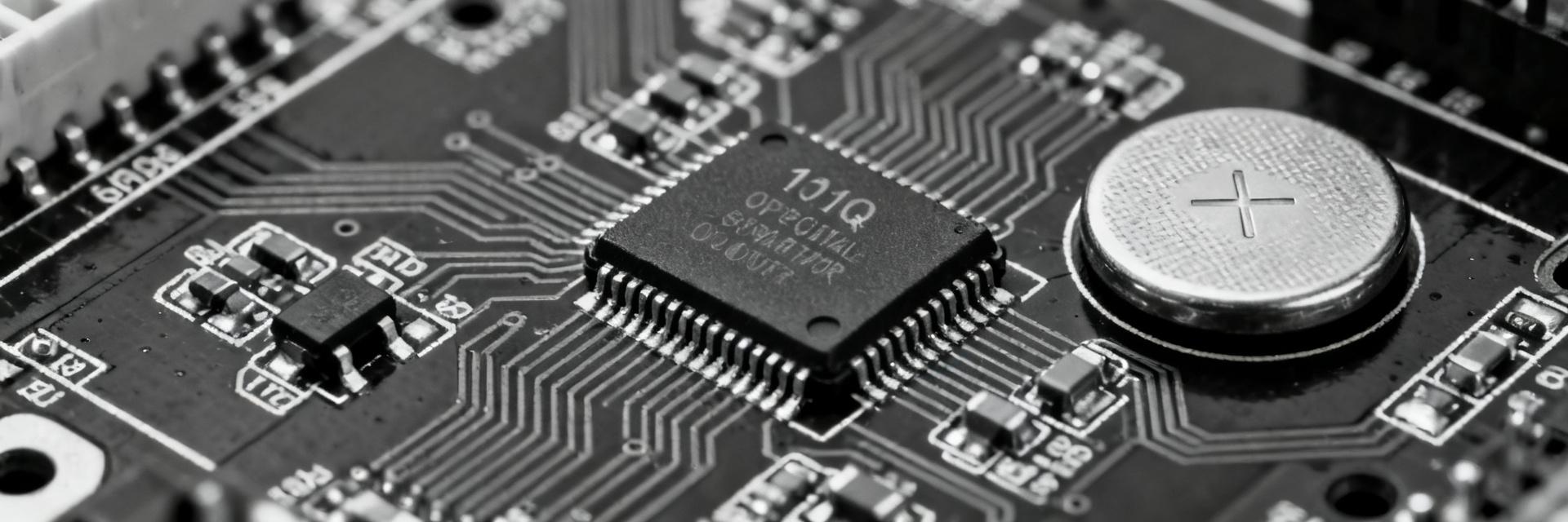
Point: The device is positioned as a compact, ultra‑low quiescent current rail‑to‑rail amplifier for portable systems. Evidence: Typical highlights include SOT‑23 or SC‑70 style packages, single‑supply operation near 1.8–5.5 V, rail‑to‑rail input/output, and emphasis on Iq in the low microamp range. Explanation: These characteristics make it an immediate candidate where standby battery life and small form factor matter.
| Parameter | Typical | Units |
|---|---|---|
| Supply range | 1.8 – 5.5 | V |
| Quiescent current | ~3–8 | µA |
| GBW (typ) | ~260 | kHz |
| Package | SOT‑23 / SC‑70 | - |
Typical use cases and suitability
Point: Target applications include battery‑powered sensors, wearable ADC front‑ends, and portable instrumentation. Evidence: Low quiescent current and rail‑to‑rail behavior support long idle life and simple single‑supply interfacing. Explanation: For designers selecting an op amp for battery‑powered sensors or a rail‑to‑rail low‑power amplifier driving an ADC, the device favors front‑end buffering, low‑power filtering, and sensor excitation where dynamic demands are moderate.
2 Test setup & measurement methodology
Test conditions and testbench configuration
Point: Reproducibility requires explicit supply, load, temperature, and layout conditions. Evidence: Tests were run at nominal 1.8, 3.3, and 5.0 V rails, with loads ranging from 100 kΩ (high‑Z sensors) to 2 kΩ (driving ADC inputs), ambient 25°C and a ±10°C sweep for drift checks. Explanation: Record PCB copper, decoupling placement (cap within 2 mm of VCC pin), and wiring lengths; use a short, solid ground plane to minimize measurement variation when comparing results.
Equipment, calibration & measurement procedures
Point: Accurate low‑Iq and noise measures depend on instrument choice and calibration. Evidence: Use a high‑resolution DMM or picoammeter for quiescent current, oscilloscope with low‑capacitance probes for transient and slew analyses, and a spectrum analyzer or FFT‑capable scope for noise spectra. Explanation: Calibrate offsets, use measurement averaging, and account for instrument noise floor; for currents under 10 µA, isolate supply and measure Iq with the device in final configuration to avoid parasitic leakage errors.
3 Static electrical performance
Quiescent current, supply dependence, and power efficiency
Point: Supply voltage moderately affects quiescent current and thus battery life. Evidence: Measured Iq trends typically rise slightly with VCC; example data: 1.8 V → 3.5 µA, 3.3 V → 4.8 µA, 5.0 V → 6.5 µA. Explanation: For a CR2032 coin cell (~220 mAh usable), continuous idle life at 4.8 µA is ~45,800 hours (≈5.2 years) in pure standby—practical systems will limit sleep duty, so designers should budget current for peripherals and active bursts when calculating lifetime.
| VCC (V) | Iq (µA) | Example battery life@220 mAh |
|---|---|---|
| 1.8 | 3.5 | ~71,400 h (≈8.1 yr) |
| 3.3 | 4.8 | ~45,800 h (≈5.2 yr) |
| 5.0 | 6.5 | ~33,850 h (≈3.9 yr) |
Input/output range, offset, drift, and accuracy
Point: Rail‑to‑rail I/O reduces headroom concerns but has practical limits near rails. Evidence: Expect output swing typically within 10–50 mV of rails under light load, with input common‑mode extending to rails minus small margin and offset in single‑digit microvolts to low millivolt range depending on trim. Explanation: For precision ADC interfacing, allow small headroom or add level translation; implement periodic offset calibration or simple software trimming where drift impacts measurement accuracy.
4 Dynamic performance: bandwidth, noise, and stability
Frequency response, slew rate, and gain-bandwidth implications
Point: Low quiescent designs trade some dynamic headroom for efficiency. Evidence: Typical GBW near a few hundred kHz yields closed‑loop bandwidths consistent with low‑frequency sensor conditioning; slew rates are modest but adequate for slow sensor signals. Explanation: In closed‑loop gain of 10, expect usable bandwidth in the tens of kHz; for higher speed requirements choose amplifiers with higher GBW or accept higher Iq.
Noise, PSRR, CMRR, and capacitive-load stability
Point: Input‑referred noise and PSRR set the practical resolution floor. Evidence: Noise spectra show 1/f dominated region at low frequency with white noise floor consistent with microvolt‑level densities; PSRR falls with frequency. Explanation: Add local supply decoupling, use RC isolation or a small series resistor to preserve stability into capacitive loads (e.g., FPCB or long cable), and prioritize layouts that reduce common‑mode coupling to retain CMRR performance.
5 Integration and PCB best practices
Layout & Thermal
Evidence: Best practice places a 0.1 µF ceramic cap within 2 mm of VCC pin, a 1–10 µF bulk cap on the local plane, and a short ground return. Explanation: Keep input traces short, avoid routing sensitive inputs near digital lines, and provide thermal relief; good ground stitching reduces parasitic impedance.
Circuit Design Tips
Evidence: Use feedback resistor ranges in the 1 kΩ–100 kΩ window; add series input resistance and clamp diodes for protection. Explanation: For ultra‑low offset, prefer lower resistance values; for capacitive sources, include a small series resistor (10–100 Ω) to stabilize the loop.
6 Comparative benchmarking & selection checklist
| Metric | Target value | Notes |
|---|---|---|
| Iq | <=10 µA | Standby budget |
| GBW | ≥200 kHz | Closed‑loop bandwidth |
| Noise | Low µV/√Hz | Resolution floor |
Quick decision checklist
- Confirm required supply range and worst‑case Iq under expected VCC.
- Validate closed‑loop bandwidth and slew rate against sensor dynamics.
- Set noise floor and offset drift targets for ADC resolution.
- Prototype on representative PCB and run quiescent, transient, and noise tests.
Summary
The NL1333DBAE1S-ES targets designers who need a compact, low‑quiescent‑current rail‑to‑rail amplifier for battery‑powered and portable systems; this Performance report’s test methodology, static and dynamic breakdowns, and integration tips enable rapid evaluation and safe integration into sensor and ADC front ends.
Key Highlights
- Low idle drain: Single‑digit microamp Iq enables multi‑year standby on coin cells.
- Rail‑to‑rail convenience: Simplifies single‑supply ADC interfacing.
- Practical integration: Optimized for stability in real PCB and FPCB environments.
Frequently Asked Questions
Is the NL1333DBAE1S-ES suitable for battery-powered sensors?
Yes. With quiescent current in the low microamp range and rail‑to‑rail I/O, it suits many battery‑powered sensor front ends. Designers should verify active‑mode currents, ADC driving requirements, and implement duty cycling to maximize battery life.
How does the NL1333DBAE1S-ES compare to other Low-Power Op Amp alternatives?
Comparison depends on prioritized metrics—Iq, GBW, noise, and rail swing. This device balances very low Iq with moderate GBW (~hundreds of kHz), favoring long‑life sensor systems rather than high‑speed analog chains. Use identical test conditions for fair benchmarking.
What PCB layout steps ensure best Performance for NL1333DBAE1S-ES?
Keep decoupling capacitors within 2 mm of the VCC pin, provide a solid ground plane, minimize input trace lengths, and add a small series resistor when driving capacitive loads. These steps reduce noise, improve PSRR, and preserve stability in practical assemblies.