STM32F417IGT6 Performance Benchmarks: Real Specs Analysis
Introduction (data-driven hook)
Point: The MCU headline numbers set an initial performance expectation.
Evidence: The device advertises a 168 MHz maximum core clock and approximately 1 MB of on-chip flash; community tests on the STM32F4 family report CoreMark and Dhrystone ranges that correlate with these figures.
Explanation: This article translates those specs into repeatable performance benchmarks and pragmatic design guidance for embedded engineers evaluating throughput, latency, and workload fit.
Point: Purpose and scope.
Evidence: We focus on single‑core, single‑threaded measurements (CoreMark/Dhrystone), memory and peripheral throughput, and reproducible test methods using common compiler settings.
Explanation: Readers will get data-driven expectations, concrete test recipes, and optimization checklists to align design choices with measured capabilities rather than datasheet peak claims.
Key specs & architecture overview (background)
Core, clock and architecture fundamentals
Point: Core features drive integer and floating-point performance.
Evidence: The MCU uses an ARM Cortex‑M4 core with single‑precision FPU and DSP extensions running up to 168 MHz; ART/cache and pipeline depth materially affect tight loops.
Explanation: The presence of an FPU and SIMD‑style DSP instructions typically improves floating‑point and signal‑processing benchmarks, while the ART accelerator reduces flash wait states for instruction fetches, raising sustained CoreMark-style throughput under typical compiler optimizations.
Memory, buses and on-chip peripherals
Point: Memory hierarchy and buses set practical bandwidth limits.
Evidence: On‑chip resources include ~1 MB flash, multiple SRAM banks, an AHB/APB bus matrix, FSMC for external memory, and a MAC for Ethernet; DMA controllers can move data with minimal CPU involvement.
Explanation: Effective performance depends on bus contention, DMA channel mapping, and whether instruction/data fetches hit ART/cache; peripheral peak rates are constrained by controller and driver overhead, not just raw interface specs.
Raw CPU performance: Dhrystone & CoreMark results
| Benchmark Type | Metric Focus | Expected Range (@168MHz) |
|---|---|---|
| CoreMark | Integer Performance / Pipeline | Mid-hundreds (Compiler dependent) |
| Dhrystone | MIPS / General Compute | ~210 DMIPS |
Expected CoreMark and Dhrystone methodology & numbers
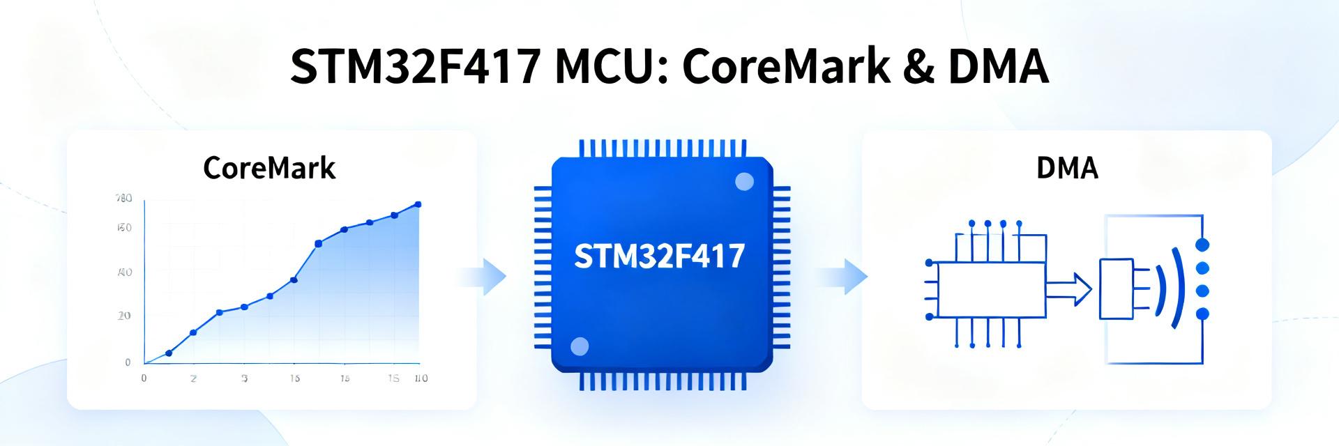
Point: Synthetic benchmarks provide repeatable baseline metrics when run under controlled builds. Evidence: Representative community CoreMark results for Cortex‑M4 devices at 168 MHz commonly fall into a mid‑hundreds range (subject to build flags such as -O2 or -Ofast and whether FPU intrinsics are enabled). Explanation: To compare apples‑to‑apples, run CoreMark and Dhrystone with fixed clock, caches enabled, and the same optimization flags; expect CoreMark to be a practical indicator for integer throughput while Dhrystone gives complementary integer/MIPS perspective.
Interpreting DMIPS/CoreMark for real workloads
Point: Synthetic scores must be converted into task budgets. Evidence: A CoreMark score divided by measured loop costs maps to available cycles per millisecond; for example, a mid‑hundreds CoreMark on a 168 MHz device means designers can budget CPU percentage for control loops, FFT sizes, or RTOS task sets. Explanation: Use benchmark scores to estimate task capacities (e.g., maximum FFT length at given sample rate) but account for I/O waits and DMA offload that synthetic tests typically exclude.
Memory & I/O throughput: real-world transfer numbers
Flash/SRAM access and DMA throughput impacts
Point: Memory access latencies and DMA strongly affect sustained performance. Evidence: ART/cached flash execution can approach zero‑wait instruction fetches for linear code; SRAM accesses are faster but limited by bus arbitration and DMA channel priority. Explanation: In practice, memcpy‑style microbenchmarks with DMA enabled reveal that internal bus throughput sustains higher block transfers than CPU‑driven copies—measure both CPU memcpy and DMA block rates to quantify real system behavior.
Peripheral throughput: Ethernet, FSMC, ADC/DMA
Point: Peripheral peak rates differ from sustained application throughput. Evidence: Ethernet MAC raw rates approach line speed in isolated tests, but TCP/IP stack overhead, IRQ handling, and driver implementation reduce practical throughput; FSMC can deliver high raw bursts to external memory or displays, while ADC with DMA streamlines sampling. Explanation: Benchmark Ethernet with an iperf‑style sustained test and FSMC with long sequential writes to reveal sustained bandwidth and latency under driver overhead.
Reproducible benchmarking methodology & test setup
Recommended tools, firmware and compile settings: Use published benchmark suites (CoreMark/Dhrystone), hardware performance counters when available, and standard compiler flags (recommended -O2 or -Ofast with explicit FPU/float ABI settings). Explanation: Build a small harness that logs timestamps over a serial port or SWO, pins markers for scope capture, and isolates the benchmark by disabling unrelated peripherals to ensure repeatable performance benchmarks across runs and boards.
Test controls: clocks, caches, power modes, and measurement pitfalls: Small configuration changes produce large measurement variance. Evidence: Enabling/disabling ART, prefetch, or power scaling changes cycle counts; background interrupts or peripheral DMA will skew results. Explanation: Verify clocks, confirm caches/prefetch state, freeze unrelated timers, and run multiple iterations; maintain a checklist (clock source and PLL, ART/cache enabled, supply voltage and regulator mode, interrupt masking, DMA off for CPU tests, serial logging buffer sizes) to ensure reproducible runs.
Comparative cases & application-level benchmarks
STM32F417IGT6 Workloads
Point: Application cases show where the MCU excels. Evidence: In real‑time FIR/FFT signal chains, FPU‑accelerated code and DMA streaming can keep CPU load under 50% for moderate FFT sizes; as an Ethernet data logger the MAC with efficient zero‑copy buffers sustains dozens to hundreds of KB/s depending on stack. Explanation: Use these case estimates to size buffers and schedule tasks.
Comparison Analysis
Point: This MCU balances DSP capability with embedded determinism. Evidence: Compared to higher‑core or higher‑memory parts, the Cortex‑M4 offers strong single‑threaded DSP and deterministic interrupts but may lose out on multi‑stream networking. Explanation: Choose STM32F4 when low latency and FPU/DSP are priorities.
Optimization checklist & design recommendations
Firmware and compiler optimizations
Point: Prioritized optimizations close the gap between datasheet and system performance. Evidence: Enabling ART/cache and prefetch, placing hot code in tightly aligned flash/SRAM regions, using DMA for bulk transfers, and linking FPU libraries often produce measurable gains versus baseline builds.
System-level tradeoffs
Point: Design must balance throughput with power and timing needs. Evidence: Lowering core voltage or switching to power modes reduces clock headroom; binding strict interrupt latency targets may preclude some aggressive DMA or cache strategies.
Summary
- Core takeaway: The STM32F417IGT6 delivers a high‑performance Cortex‑M4 foundation (168 MHz, 1 MB flash) suitable for DSP and control workloads when properly configured and benchmarked.
- Measurement guidance: Run CoreMark/Dhrystone with consistent compiler flags and ART/cache settings, then validate memory and peripheral throughput with DMA‑based microbenchmarks to expose real bottlenecks.
- Design action: Prioritize ART/cache enablement, DMA offload, and linker placement; use benchmark results to size buffers and schedule tasks for deterministic performance.
- Next step: Run the provided test templates on your dev board, compare CoreMark and I/O throughput against these estimates, and iterate with the optimization checklist.
FAQ — Performance-oriented questions
How do I reproduce STM32F417IGT6 benchmark numbers reliably?
Point: Reproducible measurements require a controlled setup. Evidence: Fix PLL/clocks, enable ART/cache, set compiler flags consistently, disable unrelated peripherals, and log timestamps for multiple runs. Explanation: Use the same toolchain and flags across experiments, run each test many times, and report median values.
What CoreMark/Dhrystone settings matter for performance benchmarks?
Point: Compiler and runtime settings strongly influence scores. Evidence: Optimization level (-O2 vs -Ofast), float ABI, and link placement determine instruction mix and cache behavior. Explanation: Use -O2 or -Ofast with the correct FPU ABI, enable inline and link time optimization where helpful, and keep hot routines in low‑latency memory.
Which tests reveal Ethernet vs FSMC bottlenecks?
Point: Use both latency and sustained throughput tests. Evidence: For Ethernet, run sustained TCP/UDP streaming tests; for FSMC, benchmark long sequential reads/writes with driver overhead minimized. Explanation: Compare raw peripheral burst rates to sustained application throughput; if sustained rates fall well below raw bursts, investigate driver, IRQ frequency, and DMA configuration.