.geo-fragment *, .geo-fragment *::before, .geo-fragment *::after { box-sizing: border-box; }
.geo-fragment {
font-family: -apple-system, BlinkMacSystemFont, "Segoe UI", Roboto, Helvetica, Arial, sans-serif;
line-height: 1.8;
color: var(--text-color, #111827);
max-width: 100%;
margin: 0 auto;
background: transparent;
}
.geo-fragment h1 { font-size: 36px; font-weight: 800; margin-bottom: 28px; line-height: 1.2; }
.geo-fragment h2 {
font-size: 26px; font-weight: 700; margin: 40px 0 20px 0;
border-left: 5px solid currentColor; padding-left: 12px;
}
.geo-fragment h3 { font-size: 20px; font-weight: 600; margin: 24px 0 12px 0; }
.geo-fragment p { margin-bottom: 1.5em; }
.geo-fragment ul { margin-bottom: 1.5em; padding-left: 1.5em; }
.geo-fragment blockquote {
margin: 20px 0; padding: 10px 20px;
border-left: 4px solid currentColor; font-style: italic; opacity: 0.9;
}
.geo-fragment table {
width: 100%; border-collapse: collapse; margin: 24px 0;
animation: geoFadeIn 0.8s forwards;
}
.geo-fragment thead th { border-bottom: 2px solid currentColor; text-align: left; padding: 12px; }
.geo-fragment td { padding: 12px; border-bottom: 1px solid rgba(0,0,0,0.1); }
@media (prefers-color-scheme: dark) { .geo-fragment td { border-bottom: 1px solid rgba(255,255,255,0.1); } }
.geo-fragment tr:hover { background: rgba(0,0,0,0.02); }
.geo-fragment svg { display: block; margin: 30px auto; animation: geoFadeIn 1s forwards; max-width: 100%; height: auto; }
.geo-fragment details { border-bottom: 1px solid currentColor; padding: 12px 0; }
.geo-fragment summary {
list-style: none; cursor: pointer; font-weight: 600;
display: flex; justify-content: space-between; align-items: center;
}
.geo-fragment summary::-webkit-details-marker { display: none; }
.geo-fragment summary::after { content: "+"; font-size: 20px; }
.geo-fragment details[open] summary::after { content: "-"; }
@keyframes geoFadeIn { from { opacity: 0; transform: translateY(10px); } to { opacity: 1; transform: translateY(0); } }
{
"@context": "https://schema.org",
"@graph": [
{
"@type": "TechArticle",
"headline": "MT29F512G08AUCBBH8-6IT:B Datasheet - Pinout & Specs",
"description": "Comprehensive guide for MT29F512G08AUCBBH8-6IT:B, a 512Gbit SLC parallel NAND in 152-pin LBGA package.",
"articleBody": "The MT29F512G08AUCBBH8-6IT:B is a 512Gbit SLC parallel NAND device offering high-density storage with 3.3V VCC and 166 MHz interface. Key for industrial integration and PCB design."
},
{
"@type": "Product",
"name": "MT29F512G08AUCBBH8-6IT:B",
"description": "512Gbit (64G x 8) SLC Parallel NAND Flash, 152-pin LBGA",
"offers": {
"@type": "Offer",
"priceCurrency": "USD",
"availability": "https://schema.org/InStock"
},
"review": {
"@type": "Review",
"author": {"@type": "Organization", "name": "FAE Team"},
"reviewRating": {"@type": "Rating", "ratingValue": "5"}
}
},
{
"@type": "FAQPage",
"mainEntity": [
{
"@type": "Question",
"name": "What are the key pinout groups for MT29F512G08AUCBBH8-6IT:B?",
"acceptedAnswer": {
"@type": "Answer",
"text": "The primary groups are VCC/VSS power, DQ[7:0] data bus, address lines, control signals (CE#, WE#, RE#, R/B#), CLK, RESET, and ZQ."
}
},
{
"@type": "Question",
"name": "Which datasheet limits are critical for PCB thermal planning?",
"acceptedAnswer": {
"@type": "Answer",
"text": "Critical limits include max junction temperature, reflow profile, and package power dissipation. Use thermal vias and copper pours."
}
},
{
"@type": "Question",
"name": "What firmware considerations should teams prioritize?",
"acceptedAnswer": {
"@type": "Answer",
"text": "Prioritize ECC selection (BCH/LDPC), wear-leveling, bad-block management, and power-loss-safe write sequencing."
}
},
{
"@type": "Question",
"name": "What is the typical interface speed and voltage?",
"acceptedAnswer": {
"@type": "Answer",
"text": "The device operates with a typical VCC of 3.3V (2.7-3.6V range) and supports interface rates up to 166 MHz."
}
}
]
}
]
}
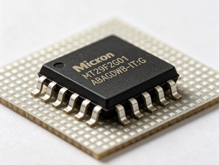
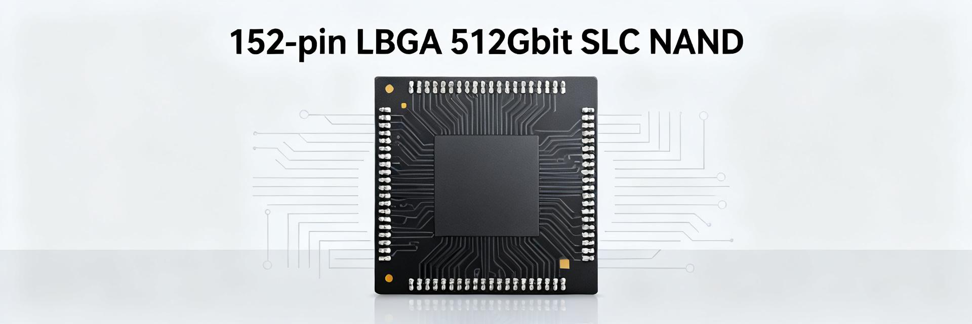
The MT29F512G08AUCBBH8-6IT:B is a 512Gbit SLC parallel NAND device (64G × 8) in a 152-pin LBGA package, offering high-density storage with a typical VCC around 3.3V and interface rates up to 166 MHz. This datasheet-oriented reference gives a quick pinout summary, key electrical characteristics, PCB and thermal guidance, integration best practices, and a ready checklist for engineers tasked with board-level integration and verification.
Device Overview & Intended Applications
MT29F512G08
152-pin LBGA
VCC/VSS
DQ[0:7]
CE#/WE#
R/B# / CLK
Thermal Via Array
Key Device Identity & Organization
The device is a 512Gbit organized as 64G × 8, single-level cell (SLC) parallel NAND in a 152-ball LBGA. This organization yields byte-wide parallel access ideal for embedded storage, boot ROM, industrial logging, and controller-resident file systems.
Capacity: 512Gbit (64G × 8)
Memory Type: SLC NAND, Parallel interface
Package: 152-pin LBGA
Typical VCC: ≈3.3 V; Interface: up to ~166 MHz
Suggested schematic-level usage: device connected to an 8-bit host bus with dedicated CE#, WE#, RE#, R/B# monitoring, and a CLK distributed to the device clock input.
Electrical Characteristics & Absolute Ratings
ParameterDesign Note
VCC RangeOperating 2.7–3.6 V; Typical 3.3 V
Max Interface RateParallel 8-bit; Max clock ≈166 MHz
Temperature RangeIndustrial Grade Support (-40°C to +85°C)
Package Type152-pin LBGA; 14 x 18mm typically
Supply, Power, and Timing Essentials
Key electrical parameters include supply ranges (commonly 2.7–3.6 V) and maximum interface frequency near 166 MHz. Pull VCC, ICC_Read/Write/Standby, tRC/tWC and max clock values into reference callouts to clarify power budgets and timing margins.
Absolute Maximum Ratings and Thermal Considerations
Verify absolute voltage and storage temperature limits. On-PCB thermal design should use thermal vias under the LBGA and large internal copper pours to ensure heat escape and reliable solder joints during reflow.
Pinout & Package Signal Groups
Pinout Summary
Organize the pinout into power, ground, address/data, and control clusters. This simplifies decoupling placement and signal routing. Ensure DQ[7:0], CE#, WE#, RE#, R/B#, CLK, ZQ, and RESET are mapped accurately to the controller.
Integration & Interfacing Best Practices
PCB Routing and Signal Integrity
Keep address and data bus traces short and uniform. Prioritize length-matching for critical control signals. Place decoupling capacitors within 0.5–1.0 mm of VCC balls and provide test points for CE#, WE#, and RE# for validation.
Power Sequencing and Reset Handling
Apply primary VCC first, then I/O VCC, assert RESET/HOLD per timing table, and only release reset after VCC stabilizes. Use a local decoupling network (0.1 µF + 10 µF bulk) per VCC ball.
Compatibility & Performance
Controller Considerations and Firmware Tips
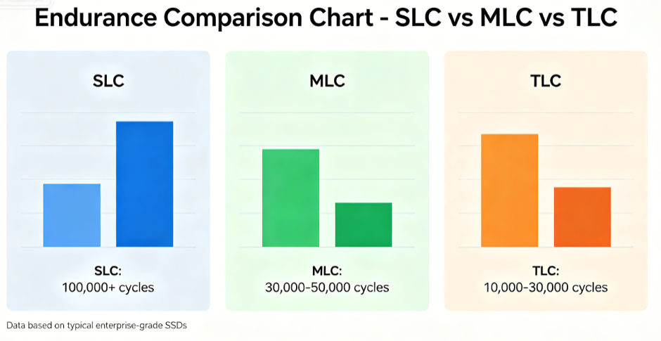
Ensure the host controller supports the parallel command set and implements BCH or LDPC ECC. Incorporate wear leveling, garbage collection, and bad-block management in the firmware layer.
Design Checklist for Engineers
Confirm 152-pin LBGA footprint against datasheet mechanical drawings.
Map all VCC and VSS balls with dedicated decoupling strategy.
Define signal length-matching requirements for the 8-bit data bus.
Validate thermal plan with vias and internal copper pours.
Set firmware ECC thresholds per SLC raw bit error rate requirements.
Common Questions
What are the key pinout groups for MT29F512G08AUCBBH8-6IT:B?
The primary pinout groups are VCC and VSS power balls, the DQ[7:0] data bus, address lines, control signals (CE#, WE#, RE#, R/B#), CLK, and special pins like RESET and ZQ. Map these groups in the schematic to ensure correct footprint and decoupling placement.
Which datasheet limits are critical for PCB thermal planning?
Critical limits include maximum junction temperature, recommended reflow profile, and package power dissipation figures. Use the mechanical drawing and thermal notes to size copper pours and thermal vias to ensure heat escape during operation.
What firmware considerations should teams prioritize for this NAND?
Prioritize ECC selection (BCH/LDPC per raw BER), wear-leveling, bad-block management, and power-loss-safe write sequencing. Validate firmware against the datasheet's command timing and error behavior tables.
What is the typical interface speed and voltage?
The device operates with a typical VCC of 3.3V (2.7-3.6V range) and supports interface rates up to 166 MHz, offering high-speed parallel data transfer.