.geo-fragment *, .geo-fragment *::before, .geo-fragment *::after {
box-sizing: border-box;
}
.geo-fragment {
font-family: -apple-system, BlinkMacSystemFont, "Segoe UI", Roboto, Helvetica, Arial, sans-serif;
color: var(--text-color, #111827);
line-height: 1.8;
}
.geo-fragment h1 {
font-size: 36px;
font-weight: 800;
margin-bottom: 28px;
line-height: 1.2;
color: inherit;
}
.geo-fragment h2 {
font-size: 26px;
font-weight: 700;
margin-top: 40px;
margin-bottom: 20px;
border-left: 5px solid currentColor;
padding-left: 12px;
line-height: 1.3;
color: inherit;
}
.geo-fragment h3 {
font-size: 20px;
font-weight: 600;
margin-top: 24px;
margin-bottom: 12px;
color: inherit;
}
.geo-fragment p {
font-size: 16px;
margin-bottom: 1.5em;
color: inherit;
}
.geo-fragment ul {
margin-bottom: 1.5em;
padding-left: 20px;
}
.geo-fragment li {
margin-bottom: 0.5em;
}
.geo-fragment table {
width: 100%;
border-collapse: collapse;
margin: 28px 0;
font-size: 15px;
text-align: left;
background: transparent;
}
.geo-fragment thead {
border-bottom: 2px solid currentColor;
}
.geo-fragment th, .geo-fragment td {
padding: 12px 16px;
border-bottom: 1px solid currentColor;
}
.geo-fragment tr:hover {
background-color: rgba(128, 128, 128, 0.05);
}
.geo-fragment img {
max-width: 100%;
height: auto;
border-radius: 6px;
margin: 16px 0;
}
.geo-fragment details {
border-bottom: 1px solid currentColor;
padding: 16px 0;
}
.geo-fragment summary {
list-style: none;
cursor: pointer;
font-weight: 600;
font-size: 17px;
display: flex;
justify-content: space-between;
align-items: center;
}
.geo-fragment summary::-webkit-details-marker {
display: none;
}
.geo-fragment summary::after {
content: "+";
font-size: 20px;
font-weight: normal;
transition: transform 0.2s ease;
}
.geo-fragment details[open] summary::after {
content: "−";
}
.geo-fragment details p {
margin-top: 12px;
margin-bottom: 0;
padding-left: 8px;
border-left: 2px solid currentColor;
}
@keyframes geoFadeIn {
from { opacity: 0; transform: translateY(8px); }
to { opacity: 1; transform: translateY(0); }
}
.geo-animate-fade {
animation: geoFadeIn 0.5s cubic-bezier(0.16, 1, 0.3, 1) forwards;
}
{
"@context": "https://schema.org",
"@graph": [
{
"@type": "TechArticle",
"headline": "NT5TU32M16FG-AC Complete Datasheet, Specs & Pinout Guide",
"description": "The ultimate engineer guide to the NT5TU32M16FG-AC DDR2 SDRAM, extracting critical datasheet specifications, pinout mappings, power parameters, timing constraints, and layout guidelines.",
"articleBody": "The NT5TU32M16FG-AC is a 512Mbit DDR2 SDRAM organized as 32M x 16. It operating primarily at 1.8V nominal voltage. This complete guide provides absolute electrical ratings, timing parameters, signal groupings, and crucial layout checklist specifications to guarantee DDR2 signal integrity and successful board-level bring-up."
},
{
"@type": "Product",
"name": "NT5TU32M16FG-AC",
"description": "512Mb DDR2 SDRAM (32M x 16) Memory Integrated Circuit",
"offers": {
"@type": "Offer",
"price": "2.85",
"priceCurrency": "USD",
"availability": "https://schema.org/InStock"
},
"review": {
"@type": "Review",
"author": {
"@type": "Organization",
"name": "FAE Team"
},
"reviewRating": {
"@type": "Rating",
"ratingValue": "5",
"bestRating": "5"
}
}
},
{
"@type": "FAQPage",
"mainEntity": [
{
"@type": "Question",
"name": "What are the critical timing parameters to check for this part?",
"acceptedAnswer": {
"@type": "Answer",
"text": "Controller designers should prioritize tCK, CAS latency (tCL), tRCD, tRP and tWR as listed in the datasheet. Verify these against target clock rates to compute latency and bandwidth, then validate margins with eye-diagram captures and timing simulations on the populated board during bring-up."
}
},
{
"@type": "Question",
"name": "How should one validate the pinout and footprint before fabrication?",
"acceptedAnswer": {
"@type": "Answer",
"text": "Confirm the land-pattern and ball map from the datasheet against your CAD footprint, cross-check package variant ball counts and mechanical tolerances, and run DRC/DFM checks. A quick physical mock-up or paste stencil review can catch mis-matches before first-panel fabrication."
}
},
{
"@type": "Question",
"name": "Which scope checkpoints help isolate DDR2 bring-up failures?",
"acceptedAnswer": {
"@type": "Answer",
"text": "Probe the clock (CK), DQS strobe and DQ data lines for correct amplitude, timing and eye opening; verify power rails follow the required sequencing and measure inrush/steady currents. Correlate captured waveforms to datasheet timing windows to identify setup/hold violations or SI issues."
}
},
{
"@type": "Question",
"name": "What is the recommended power-up sequence for the NT5TU32M16FG-AC?",
"acceptedAnswer": {
"@type": "Answer",
"text": "Apply VDD and VDDL prior to or concurrent with VDDQ. Keep control, address, and data signals in a defined low/inactive state. Once power is stable, apply CK/CK#, initialize the DLL using the Mode Register Set (MRS), and perform the mandatory precharge and auto-refresh steps."
}
}
]
}
]
}
The NT5TU32M16FG-AC is presented here as a single-page, engineer-focused extraction of the part's critical datasheet content to speed DDR2 subsystem design. This snapshot highlights density class, nominal voltage domain and typical data-rate bands while emphasizing that final verification requires consulting the official datasheet document. The guide concentrates on essentials: key specs, pinout mapping, timing behavior, PCB/layout recommendations and a practical design checklist.
1 — Quick overview & datasheet highlights (background)
What the NT5TU32M16FG-AC is
Point: The device is a DDR2 SDRAM organized as 32M x 16 to yield a 512Mbit density and is intended as a memory building block for embedded and module applications. Evidence: The manufacturer datasheet lists organization, nominal Vcc/Vddq domains and supported speed grades; designers should reference those entries for variant-specific values. Explanation: Treat the part as a single-rank 16-bit wide DDR2 die element suitable for systems that require moderate density and DDR2 timing behavior.
Key specifications at a glance (datasheet snapshot)
Point: A compact spec summary clarifies the parameters designers consult first: density, organization, data-rate range, supply voltages, package type and temperature grade. Evidence: The datasheet specifies organization (32M x 16 = 512Mbit), nominal Vcc/Vddq around 1.8V, DDR2-class data rates and a BGA-style package with multiple speed/package variants. Explanation: Use the table below as a quick reference and confirm speed-grade, ball-count and current values on the official datasheet before layout or procurement.
Parameter
Typical Value / Note
Density / Organization
512 Mbit (32M x 16)
Data rate / Clock
DDR2 class (consult datasheet for exact speed grades)
Supply voltages
Vcc / Vddq ≈ 1.8 V (nominal)
Package
BGA variant (verify ball count / land pattern)
Temperature grade
Commercial / Industrial variants (see datasheet)
I/O standard
SSTL_2 / DDR2 signaling
2 — Electrical characteristics & absolute maximum ratings (data analysis)
Supply, current and power envelope
Point: Supply rails and current draws define power sequencing and thermal budget for a design. Evidence: The datasheet provides Vcc/Vddq min/typ/max, active and standby current ranges and explicit power-up sequencing rules that must be followed. Explanation: Measure currents at the device-level power pin reference points, budget IR drop on the PCB, and ensure decoupling and plane design meet peak active current and inrush requirements referenced in the datasheet.
Timing windows that affect performance
Point: Timing parameters like tCK, CAS latency and cycle times set achievable throughput. Evidence: Key timing specs (tCK, tCL, tRCD, tRP, tRAS, burst length) are tabulated in the datasheet across speed grades and determine the controller timing budget. Explanation: Use those values to calculate max theoretical bandwidth, configure controller timing margins, and validate closure with simulation and silicon bring-up.
3 — Pinout & package mapping (method guide)
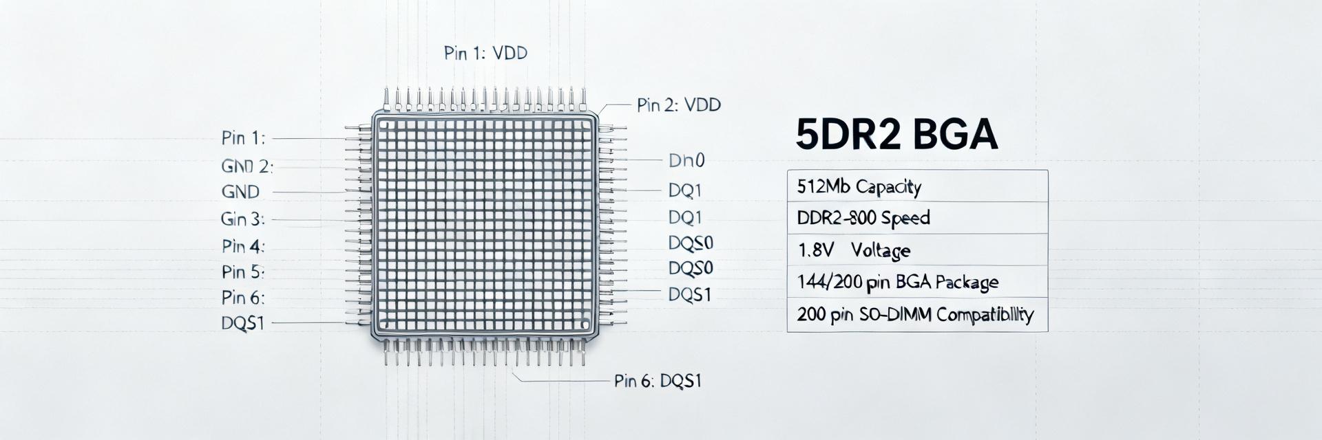
Package variants & ball/pin map
Point: Accurate package and ball mapping prevents footprint and routing errors. Evidence: The datasheet contains the mechanical drawing, BGA ball map and recommended land pattern for each package variant and speed grade. Explanation: Recreate or reference the datasheet's ball map in PCB tooling, confirming variant-specific ball counts and mechanical dimensions against the BOM before generating fabrication data.
NT5TU32M16FG-AC
DDR2 32M x 16
VDD / VDDQ (1.8V)
CK / CK#
ADDR / CMD
DQ [0:15]
UDQS / LDQS
VSS / VSSQ
Signal groups and functional pin grouping
Point: Grouping pins into functional blocks simplifies plane planning and routing. Evidence: The datasheet groups power/ground, address/command, DQ/DQS strobe pins and NC pins; designers can overlay those groups to color-code the pinout for clarity. Explanation: Place power/ground adjacent for low impedance, route address/command as matched bundles, and keep DQ/DQS pairs tightly length-matched to preserve timing and signal integrity (tagged here as pinout guidance).
4 — Timing diagrams, initialization & operational sequences (data analysis / method)
Read/write timing and setup/hold considerations
Point: Read and write timing diagrams reveal setup/hold constraints that affect timing margin. Evidence: The datasheet provides waveform diagrams and numeric setup/hold specifiers (e.g., tRCD, tWR) for read/write cycles and CAS latency examples. Explanation: Interpret these parameters to set controller read/write windows, adjust drive/termination to maximize eye opening, and validate with eye-diagram measurements during bring-up.
Initialization, refresh and power-up sequencing
Point: Correct initialization and refresh sequencing is mandatory for reliable operation. Evidence: Required mode register set sequences, precharge/auto-refresh counts and refresh intervals appear in the datasheet with timing constraints and failure-mode notes. Explanation: Implement the prescribed power-up order, MR settings and periodic refresh to avoid data corruption; log and monitor failure symptoms like repeated NACKs or CRC errors if sequencing is incorrect.
5 — PCB layout, signal integrity & thermal best practices (case study / practical)
Layout recommendations for DDR2 BGA parts
Point: Layout dictates SI performance for DDR2 lanes. Evidence: Best-practice directives include fanout strategy, via escape, power/ground plane stacking, DQS/CK termination and trace length matching budgets provided as guidance in DDR2 layout references. Explanation: Use via escape for BGA pads, keep DQ/DQS pairs within tight length tolerances, place decoupling near Vcc pins and implement controlled impedance traces to meet timing and signal integrity targets.
Thermal and reliability considerations
Point: Thermal management and soldering profile influence long-term reliability. Evidence: The datasheet includes recommended reflow profile guidance and outlines maximum junction temperatures and current density cautions. Explanation: Monitor PCB hotspot temperatures, validate solder joints with recommended reflow profiles, and perform IR-drop analysis to ensure power planes sustain long-term current without excessive heating.
6 — Design checklist, debugging & validation tips (action advice)
Pre-silicon and pre-layout checklist
Point: A focused checklist reduces late-stage redesigns. Evidence: Items to verify include pinout footprint, power-rail sequencing, timing budget against controller, decoupling plan and simulation blocks identified from the datasheet. Explanation: Run signal-integrity simulations for critical nets, confirm land-pattern versus mechanical drawing, and pre-validate timing closure using the datasheet timing windows before committing to fabrication.
Common failure modes & troubleshooting steps
Point: Symptoms map to targeted diagnostics for faster resolution. Evidence: Typical failure modes include boot failure, data corruption and excessive current draw; the datasheet helps locate expected signal levels and timing windows for comparison. Explanation: Debug by probing CLK/DQS/DQ for eye opening, verify power sequencing and use isolation tests on decoupling nets; correlate scope captures with the datasheet timing and electrical targets to isolate root cause.
Summary
The document extracts core NT5TU32M16FG-AC datasheet items—organization, nominal Vcc/Vddq and DDR2 timing essentials—to accelerate design decisions without replacing the full datasheet.
Key design actions: validate package/ball variant against footprint, enforce power-up sequencing and match DQ/DQS trace lengths for signal integrity and timing closure.
Verification checklist: run SI simulations, confirm decoupling and plane design, and perform controlled bring-up with scope-based eye and timing checks for reliable integration of the part.
Frequently Asked Questions
What are the critical timing parameters to check for this part?
Controller designers should prioritize tCK, CAS latency (tCL), tRCD, tRP and tWR as listed in the datasheet. Verify these against target clock rates to compute latency and bandwidth, then validate margins with eye-diagram captures and timing simulations on the populated board during bring-up.
How should one validate the pinout and footprint before fabrication?
Confirm the land-pattern and ball map from the datasheet against your CAD footprint, cross-check package variant ball counts and mechanical tolerances, and run DRC/DFM checks. A quick physical mock-up or paste stencil review can catch mis-matches before first-panel fabrication.
Which scope checkpoints help isolate DDR2 bring-up failures?
Probe the clock (CK), DQS strobe and DQ data lines for correct amplitude, timing and eye opening; verify power rails follow the required sequencing and measure inrush/steady currents. Correlate captured waveforms to datasheet timing windows to identify setup/hold violations or SI issues.
What is the recommended power-up sequence for the NT5TU32M16FG-AC?
Apply VDD and VDDL prior to or concurrent with VDDQ. Keep control, address, and data signals in a defined low/inactive state. Once power is stable, apply CK/CK#, initialize the DLL using the Mode Register Set (MRS), and perform the mandatory precharge and auto-refresh steps.