MT40A512M16TB-062E DDR4 SDRAM: Full Specs & Analysis
Measured at up to 2400 MT/s and organized as 512M x 16, the MT40A512M16TB-062E represents a widely used 8Gbit DDR4 SDRAM option for high-density parallel-memory designs. This article delivers a datasheet-backed breakdown of MT40A512M16TB-062E specs, performance analysis, design guidance, and a practical integration checklist for engineers evaluating a DDR4 memory device.
The content that follows synthesizes the part identity, key electrical and timing considerations, throughput calculations, PCB and thermal integration notes, comparison guidance, and a pre-deployment troubleshooting checklist aimed at pragmatic system design and validation.
#1 — Background & Part Overview
Part identity and configuration
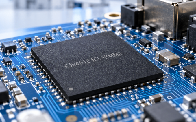
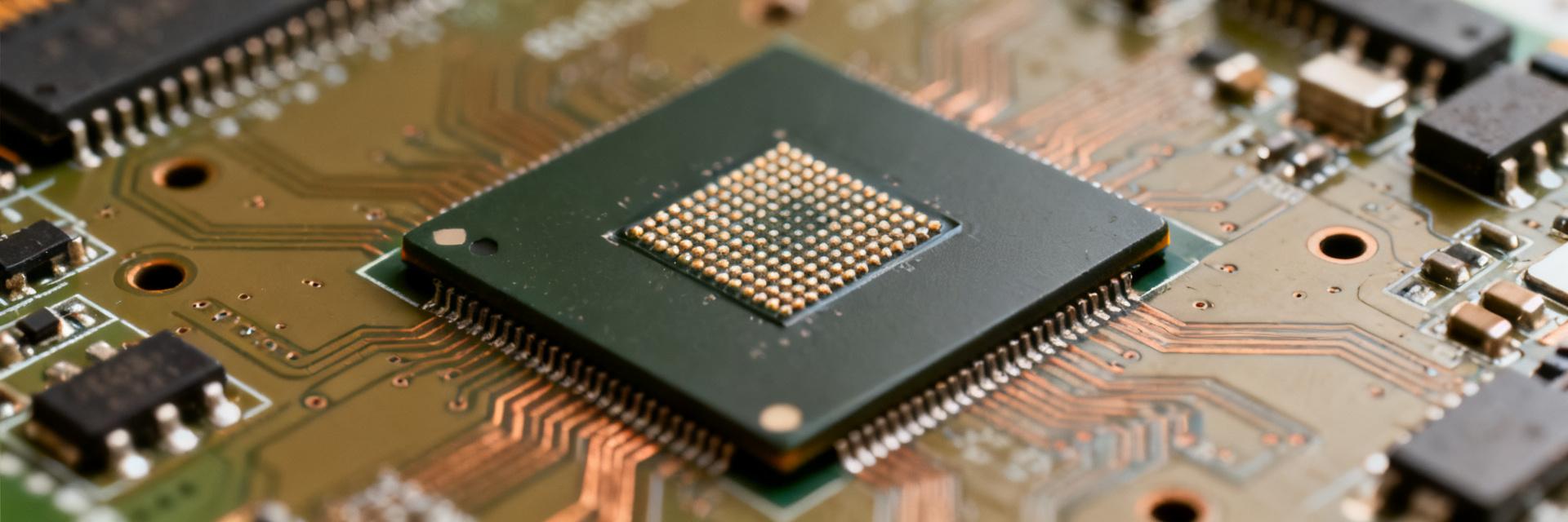
The MT40A512M16TB-062E decodes to an 8Gbit device organized as 512M x16 with a parallel DDR4 interface and an FBGA-96 package. The part is specified at a rated data rate of 2400 MT/s and uses the DDR4 nominal VDD (typical 1.2V) supply domain. The official datasheet should be consulted for absolute min/max voltages and package drawing tolerances before layout sign-off.
| Parameter | Value (summary) |
|---|---|
| Density / Organization | 8Gbit / 512M x16 |
| Data rate | Up to 2400 MT/s |
| Nominal VDD | 1.2 V |
| Package | FBGA-96 |
| Typical use | Parallel DDR4 memory arrays |
Intended applications & product lifecycle status
This class of device targets servers, networking NICs, storage controllers, and embedded compute modules that require wide parallel DDR4 x16 buffers. Because lifecycle and availability can change, engineers must check current sourcing and formal obsolescence notices from the manufacturer and capture lot traceability as part of procurement risk mitigation. Search terms to include in design documentation: "MT40A512M16TB-062E datasheet pinout".
#2 — Key Electrical & Timing Specs
Electrical characteristics
Primary electrical domains center on the DDR4 core VDD and the I/O VDDQ; the nominal core voltage is 1.2V with defined absolute min/max and I/O tolerance windows in the official datasheet. Standby and active currents vary by speed grade and operating mode; those currents should be copied verbatim from the datasheet into the board power budget. Voltage tolerance and sequencing matter for regulator selection and level-shifter design when multiple supply rails or legacy I/O voltages exist.
Timing and reliability parameters
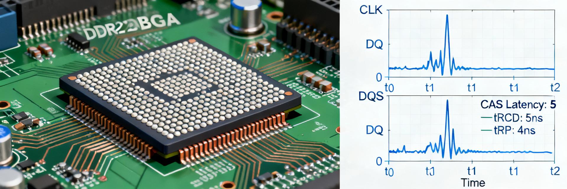
Key timing parameters to record from the datasheet include supported data rate (2400 MT/s), clock frequency, supported CAS latencies, tRCD, tRP, tRAS, refresh interval, and cycle timing windows. Include reported ECC behavior, thermal derating notes, and any specified BER or reliability metrics. For formal timing sign-off, place the manufacturer timing table directly into the design pack and treat refresh and retention tables as design constraints.
#3 — Performance Benchmarks & Throughput Analysis
Theoretical bandwidth & calculation walkthrough
Peak theoretical throughput per device is computed as: data rate (transfers/s) × bus width (bits) ÷ 8 = bytes/s. For 2400 MT/s on a 16-bit interface: 2400e6 × 16 ÷ 8 = 4.8e9 bytes/s, or roughly 4800 MB/s per device. Multiple parallel devices or multiple channels scale aggregate bandwidth linearly in ideal conditions, so two devices in parallel yield ~9.6 GB/s theoretical peak, assuming the memory controller and interconnects scale without contention.
Real-world performance factors
Practical throughput is limited by memory controller scheduling, CAS/command timing, PCB signal integrity, rank interleaving, thermal throttling, and system-level bottlenecks such as CPU or DMA throughput. Benchmark using sustained bandwidth and latency tests that capture sequential versus random access patterns; record metrics such as sustained MB/s, 95th-percentile latency, and page-hit ratios. Use these metrics to correlate observed behavior with timing/board-level changes.
#4 — Integration & Design Considerations
PCB, routing and signal-integrity checklist
For DDR4 parallel x16 routing: implement tight trace length matching within a byte lane and between lanes where required, control differential and single-ended impedance, minimize via stubs, and apply recommended termination topologies. Follow the datasheet power-sequencing order for VDD/VDDQ and contact the official JEDEC guidance for decoupling ranges. Action items: verify BGA footprint, confirm ball map, and populate decoupling capacitors per the recommended values copied from the datasheet.
Datasheet values to copy: electrical table, timing table, power sequencing, package drawing, recommended decoupling.
Thermal, packaging and test considerations
FBGA packages require attention to thermal conduction through the board: plan copper pours, thermal vias under the BGA where allowed, and verify solder reflow profile before production. Include in-system test hooks for DDR training logs (controller training traces) and provide JTAG or equivalent access for in-field diagnostics. Recommended inspection tests include boundary-scan validation and functional memory training under worst-case temperature and voltage conditions.
#5 — Use Cases & Comparative Case Study
Typical system profiles
Profile A: An enterprise NIC uses on-board parallel DDR4 as packet buffering; primary constraints are sustained bandwidth and deterministic latency, making the 8Gbit/512M x16 organization a fit when combined with high-speed controller logic. Profile B: An embedded compute module needs a low-power DDR4 buffer for imaging pipelines—the device's nominal 1.2V operation supports efficient power use, with thermal plan and standby currents determining battery sizing.
Comparison & substitution guidance
When comparing alternatives, match density, bus width, data rate, voltage, package, and timing spec tables. For near-drop-in replacements, ensure pinout compatibility and re-run memory controller timing and signal integrity checks. Requalification steps should include full training cycles, thermal cycling, and ECC validation if used in production.
#6 — Practical Pre-deployment Checklist & Troubleshooting
Pre-deployment BOM and validation checklist
Checklist: confirm datasheet values (electrical, timing, package), verify PCB footprint and BGA ball map, power sequencing and decoupling sign-off, SI and return-loss simulations, thermal plan, and procurement lot traceability. Copy the datasheet electrical and timing tables into the design pack and include them in your formal design review and test plan documentation.
Common failure modes and debug steps
Typical failures: failed DDR training, ECC error bursts, timing violations, signal reflections, and thermal-induced errors. Debug priority: 1) capture DDR training logs from the controller, 2) scope data and command lines for eye and timing margins, 3) check power rail sequencing and noise, and 4) analyze ECC single-bit versus multi-bit patterns to isolate SI vs device issues. Quick mitigations include tightening terminations, shortening traces, and improving decoupling.
Summary
- The MT40A512M16TB-062E delivers an 8Gbit DDR4 SDRAM option organized as 512M x16 and rated to 2400 MT/s; engineers should copy the manufacturer timing and electrical tables directly into the design pack for accurate power and timing budgeting.
- Key design checks include strict trace length matching, controlled impedance routing, correct power sequencing, and an explicit thermal dissipation plan; these steps address the most common integration gotchas and enable predictable memory training and performance.
- Before deployment, validate BOM traceability, perform SI and thermal sign-off, execute DDR training capture, and run ECC stress tests; these actions reduce field failures and accelerate qualification for systems using this DDR4 device.
#常见问题 (FAQ)
What power sequencing is required for DDR4 devices?
Power sequencing typically requires VDD (core) and VDDQ (I/O) to ramp in the manufacturer-specified order with defined rise times and tolerances. Always copy the exact sequence and timing windows from the official datasheet into the board power-up procedure to avoid latch-up or training failures. Validate with power-supply margin testing under worst-case conditions.
How should engineers benchmark real-world DDR4 throughput?
Benchmark both sequential and random workloads using sustained read/write tests, capture average and tail latencies, and measure 95th/99th-percentile latency. Use platform tools that report per-channel bandwidth and latency and run tests across temperature and voltage corners to reveal throttling and controller scheduling effects.
What are first-line diagnostics for failed DDR training?
Start with controller training logs to identify which timing window failed, then probe DQ/CK/command lines for eye closure and reflections. Check power rails for noise or incorrect sequencing, verify BGA solder integrity, and attempt controlled down-clocked training to isolate margin issues before hardware respin.
What is the theoretical peak bandwidth of the MT40A512M16TB-062E?
The theoretical peak bandwidth of the MT40A512M16TB-062E is computed as: 2400 MT/s × 16 bits / 8 = 4.8 GB/s (4800 MB/s) per device. In a dual-channel or parallel configuration, this scales accordingly, yielding up to 9.6 GB/s for two devices in parallel under ideal controller scheduling conditions.