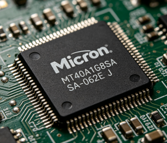
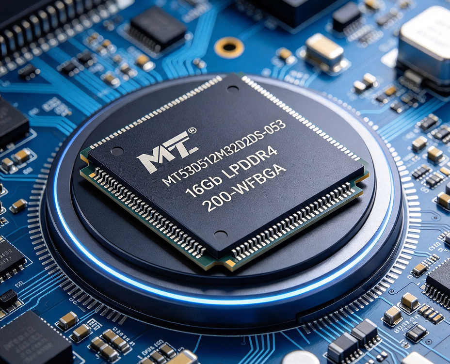
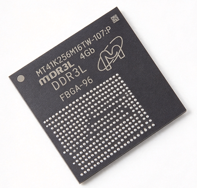
MT40A1G8SA-062E DDR4 - Full Specification and Pinout Report
Key points: The MT40A1G8SA-062E is an 8 Gbit DDR4 SDRAM with a 1G × 8 organization, rated for operating frequencies up to 3200 MT/s and a nominal supply voltage of 1.2 V. It is a compact, high-bandwidth chip suitable for embedded and board-level storage designs. Evidence: These key parameters are clearly specified in the device's datasheet. Explanation: This report summarizes device specifications, pinout, timing characteristics, PCB design guidelines, and procurement verification information for designers' reference.
Key points: Aimed at providing the layout design and firmware development teams with a single, actionable source of reference. Evidence: During the design verification phase, engineers should cross-check each numerical limit against the DDR4 datasheet (device version) provided by the vendor. Explanation: Please use the pinout table and timing summary below as the initial input for PHY configuration, signal integrity simulation, and procurement validation.
1 → Overview and Key Specifications (Background)
Device Organization Structure and Capacity
Key points: The device's organization structure is clearly marked as 1G×8, thus its density is 8 Gbit. Evidence: The datasheet indicates "1G×8" in the package chip organization section. Explanation: This organizational structure means each chip has an 8-bit-wide data bus; when configuring Rank and Channel, designers must map the device density into the controller's address/row/column calculations.
Electrical Parameter Overview and Supported Rates
Key points: The nominal VDD/VDDQ is 1.2 V, and the device supports a maximum speed grade of 3200 MT/s. Evidence: The DDR4 datasheet's speed/grade table lists 3200 MT/s as the highest supported transfer rate and provides typical CAS latency ranges. Explanation: Target timing and thermal budgets should be set around the 1.2 V operating voltage, and the selected speed grade's corresponding CL/tCK combination should be confirmed according to the datasheet.
2 → Electrical Characteristics and Timing Parameters (Data Analysis)
DC Characteristics and Power Supply
Key points: Verify Vmin/Vmax, Idd in standby and active states, and VREF requirements directly from the datasheet. Basis: The datasheet specifies a nominal VDD = 1.2 V, with VREF ≈ VDD/2; the device table provides Idd ranges for both standby and active modes. Note: Plan local decoupling near the VDD/VDDQ solder balls, follow the recommended VREF decoupling scheme, and mark any non-standard DC limits before prototyping to facilitate power consumption budgeting.
AC Timing and Performance Parameters
Key points: The critical timing parameters that need to be extracted include tCK, CL, tRCD, tRP, tRAS, tRFC, tFAW, tWR, and tWTR. Basis: At 3200 MT/s, tCK is approximately 0.625 ns; the CAS latency at this rate typically falls within the JEDEC standard range (see the datasheet table). Explanation: Use the timing tables from the datasheet to populate the PHY timing registers, and verify them using the timing tables in the SI tool.
| Parameters | Example @3200 MT/s | Reference JEDEC Standard |
|---|---|---|
| tCK (Clock Cycle Time) | ≈ 0.625 ns | DDR4-3200 (CL = 22) |
| CAS Latency (CL) | Typical Range (22-22-22) | See the manufacturer's datasheet table |
| tRCD / tRP | Configured according to JEDEC/speed grade | 13.75 ns (nominal value) |
| tRFC (Refresh Cycle Time) | 350 nanoseconds (8 Gbit density) | Standard Refresh Recovery Boundary |
3 → Pin Arrangement, Package, and Mechanical Details (Data Analysis)
Pin Arrangement Diagram and Signal Grouping
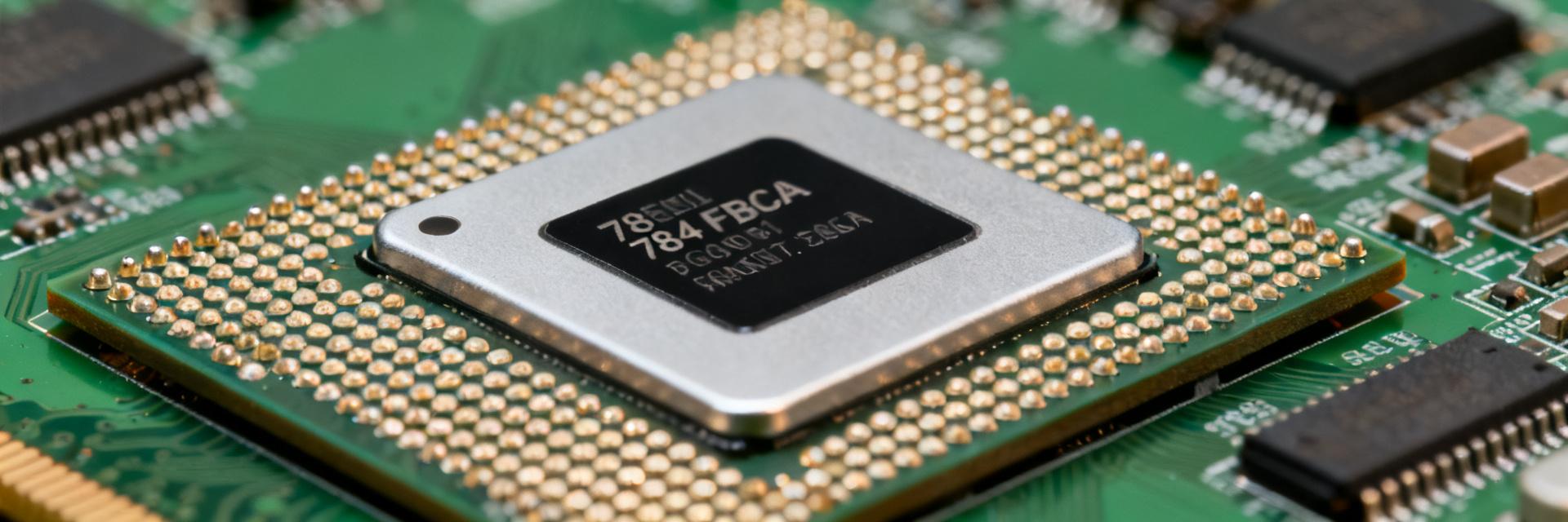
Key Points: This device uses a 78-ball FBGA package, with signal groups including: DQ, DQS/DM, CK/CK#, CA/Address and Command, BA, CKE, ODT, VSS, VDD, and NC. Basis: The package pin mapping table in the datasheet lists each solder ball number and network name, facilitating quick cross-referencing. Note: Provide the layout team with an annotated pin arrangement CSV file, ensuring that during layout design, the grouping of DQS/DQ matches the controller channel assignments.
Package Dimensions, Pad Layout, and Thermal Management Instructions
Key points: Please design according to the FBGA dimensions, pad patterns, and thermal vias recommended in the mechanical drawings. Basis: The mechanical section provides the package's X×Y dimensions, ball pitch, and recommended PCB pad tolerances. Note: Design thermal vias beneath exposed copper areas as per the drawings, adhere to the Z-stack height constraints, and confirm component placement pitch with the assembly manufacturer.
4 → PCB Routing and Signal Integrity Best Practices (Methodology Guide)
Routing, Termination, and Impedance Control
Key points: For DQ/DQS and CK networks, controlled impedance must be maintained, and strict length matching is required. Recommendation: The target single-ended impedance for DQ is approximately 40–60 ohms, and the lengths of DQ and DQS pairs should be matched; minimize short traces and follow ODT guidelines. Note: When applicable, use differential pairs to transmit CK/CK# signals, match DQS capture timing with DQ within the specified ppm range, and verify through SI simulation before tape-out.
Power Distribution and Decoupling Strategy
Key points: The PDN must place local decoupling capacitors near the VDD/VDDQ solder balls and employ a layered capacitor network. Rationale: According to the datasheet and PDN best practices, use both 0.01–0.1 µF (high-frequency) and 4.7–47 µF (large-capacitance) capacitors near the device's power pins, along with a VREF capacitor. Note: Place decoupling capacitors within 2–4 mm of the power pins, lay out wide copper planes, and verify through PDN impedance scanning corresponding to the switching frequency.
5 → Integrated Checklist: Firmware, PHY Training, and Validation (Methods/Cases)
PHY/Controller Configuration and Training Process
Key points: Use the PHY register timing, ODT, drive strength, and VREF calibration as initial reference points. Basis: Typical training content includes CK calibration, read/write equalization, and DQ/DQS alignment; PHY vendor guides already provide example register preset values (which can serve as a starting point). Note: Example values should be considered provisional—during product debugging, always verify the exact register settings against the datasheet and the PHY vendor's recommendations.
Validation Testing and Acceptance Criteria
Key points: Prioritize JEDEC compliance, read/write scans, BERT, eye diagram margin, thermal cycling, and retention characteristic checks. Basis: Acceptance criteria should be based on the timing margins and signal integrity eye diagram targets specified in the datasheet; zero uncorrected ECC errors are required during testing. Note: Automated test sequences should be run under full process, voltage, and temperature (PVT) conditions, recording margin variations, and ensuring that the specified timing margins are met before final sign-off.
6 → Procurement, Device Variants, and Compliance Checks (Action Recommendations)
Identifying Suffixes, Lifecycle, and Cross-References
Key Points: When placing orders, interpret the suffixes for speed, temperature grade, and package. Basis: Component markings and ordering codes in the datasheet can identify package type, speed grade, and temperature range—please verify against the bill of materials. Explanation: Before replacing cross-references, confirm package dimensions and pin compatibility, and request a revised datasheet from the supplier to ensure traceability.
Compliance, RoHS, and Obsolescence Verification
Key Points: Before procurement, confirm RoHS/REACH declarations, JEDEC compliance levels, and product lifecycle status. Basis: Compliance information and version notes should be indicated in the datasheet or supplier documentation; distributors can provide traceability documents. Explanation: During supplier qualification, obtain compliance certificates and the latest version of the datasheet to avoid outdated inventory or non-compliant products.
Conclusion
Key points: The MT40A1G8SA-062E is an 8 Gbit DDR4 device (1Gx8), supporting up to 3200 MT/s at 1.2 V, and packaged in a 78-ball FBGA. Basis: Key specifications and pin assignments are listed in the device datasheet and pinout table. Note: Designers should refer to the DDR4 datasheet and the aforementioned pinout table as authoritative references for layout, PHY configuration, and procurement.
Key Summary
- Device: MT40A1G8SA-062E — 8 Gbit, with a 1G x 8 organization; please use the organization string from the datasheet to accurately map memory addressing and Rank.
- Electrical and Timing: Nominal VDD/VDDQ = 1.2 V; target rate up to 3200 MT/s; parameters such as tCK, CL, tRCD, tRP, and tRFC are extracted from the PHY configuration table in the DDR4 datasheet.
- Layout and Verification: The 78-ball FBGA package requires grouped routing of DQ/DQS signals, impedance control, local decoupling, and completion of full PHY training along with JEDEC standard verification testing.
Frequently Asked Questions
What is the organization and capacity of the MT40A1G8SA-062E?
Answer: This device uses a 1G×8 organization, with a storage density of 8 Gbit. Based on the organization string in the datasheet, calculate the Rank, column address, and row address mappings, and determine how many chips are required per Rank at the target bus width.
To achieve a rate of 3200 MT/s, which timing parameters do I need to load into the PHY?
A: According to the speed grade timing tables in the datasheet, fill in parameters such as tCK, CAS (CL), tRCD, tRP, tRAS, tRFC, tFAW, tWR, and tWTR. Start with example registers provided by the PHY vendor, then during training, optimize based on the timing margins observed from eye diagrams and bit error rate tests.
What PCB design specifications can ensure signal integrity for this 78-ball FBGA?
A: Maintain a single-ended impedance of 40–60 Ω for DQ, strictly match the lengths of DQ and its associated DQS within the group's budget, minimize stubs, set terminations or use ODT as recommended in the datasheet, and place local decoupling capacitors near the VDD/VDDQ pads. Finally, verify through signal integrity (SI) and power integrity (PDN) simulations.
What are the nominal power supply requirements and decoupling recommendations?
A: The nominal operating voltage is VDD = VDDQ = 1.2V, and the specified value for VPP is 2.5V. For decoupling, a local array of high-frequency MLCC capacitors (0.01 µF to 0.1 µF) should be placed within a 2–4 mm area around the VDD/VDDQ power pins, supplemented by chip-type large-capacitance capacitors ranging from 4.7 µF to 47 µF.