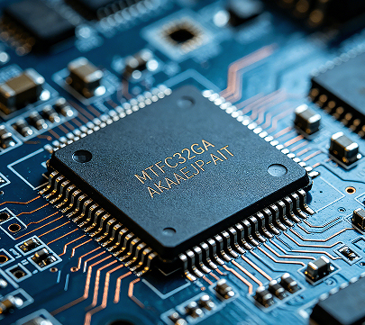
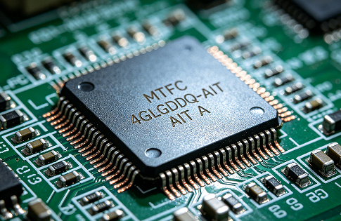
• MTFC4GLGDQ-AIT A eMMC: Specs & Performance Deep Dive

    → Introduction Datasheet figures and independent benchmarks place this part in the low‑tens of MB/s for sequential throughput and single‑digit MB/s for sustained writes under typical embedded workloads—numbers that determine suitability for many automotive and industrial systems. This article explains what the MTFC4GLGDQ-AIT A eMMC offers, how it behaves in real workloads, and practical guidance for integration and validation. Top-line specTypical value / note Capacity4 / 8 / 16 / 32 Gbit (Density-dependent) InterfaceeMMC Automotive Grade (v4.41), 8-bit bus Typical Sequential R/WRead ~25–30 MB/s, Write ~6–8 MB/s Package / TempLBGA / -40°C to +85°C (AIT Grade) eMMC Controller VCC DAT[0-7] CMD/CLK NAND → 1 — eMMC Background & System Fit 1.1 — Standard Context The MTFC4GLGDQ-AIT A utilizes a managed NAND architecture where the internal controller handles ECC, wear leveling, and bad‑block management. As a v4.41 family device, it provides a stable, long-lifecycle solution for systems that do not require the higher power draw and complexity of UFS or newer eMMC 5.1 HS400 modes. Host ←––– eMMC controller (boot region / RPMB / user area) –––→ NAND → 2 — Key Specs Breakdown The part is supplied in an LBGA package and supports 8‑bit parallel data paths. Supply rails include standard VCC (NAND core) and VCCQ (I/O) domains. Engineers should prioritize signal integrity for the CMD/DAT traces, ensuring controlled impedance to match the automotive host controller's drive strength. → 3 — Performance Deep-Dive MetricDatasheet TypicalExpected Steady‑State Sequential Read~25–30 MB/s~20–28 MB/s Sequential Write~6–8 MB/s~4–7 MB/s Random 4K IOPS~500–3000~200–1500 3.1 — Benchmark Methodology To validate real-world performance, use the following fio profiles: # Sequential Write Test fio --name=seqwrite --filename=/dev/mmcblk0 --bs=128k --iodepth=1 --rw=write --size=1G --runtime=120 # Random 4K Write Test fio --name=rand4k --filename=/dev/mmcblk0 --bs=4k --iodepth=4 --rw=randwrite --size=2G --runtime=300 → 4 — System Integration & Reliability Active R/W currents spike significantly. Design PMIC rails for transient bursts and implement thermal vias under the LBGA package. High temperatures accelerate NAND wear; implement telemetry to monitor erase/write counters and spare block counts to trigger maintenance before end-of-life. → 5 — Pre-deployment Checklist Acceptance: Confirm part markings, firmware revision, and run short fio sanity tests. Thermal: Perform a thermal soak test to catch marginal devices in the lot. Lifecycle: Track PCN (Product Change Notices) for NAND generation migrations. → Summary Reliable read performance (~25-30 MB/s) ideal for boot and firmware storage. Automotive Grade (-40°C to +85°C) ensures stability in harsh environments. Requires robust thermal management and 8-bit bus configuration for peak efficiency. → Frequently Asked Questions What are realistic IOPS for the MTFC4GLGDQ-AIT A? Realistic 4K random IOPS are typically in the low hundreds to low thousands (200-1500) depending on queue depth and the state of internal garbage collection. How do you benchmark this eMMC for steady-state performance? Use long-duration runs (minutes) with fio to account for internal controller overhead. Compare fresh-out-of-box runs against sustained write states to reveal performance degradation. What is the critical checklist for incoming eMMC lots? Validate part markings, firmware revision, capacity reporting, and perform short performance sanity tests. Enforce pass/fail thresholds based on ±20% of datasheet typicals. What are the power and thermal requirements for integration? Design PMIC rails for high-current transient R/W bursts. Use thermal vias and copper pours to manage heat, as prolonged high temperatures reduce data retention and endurance.
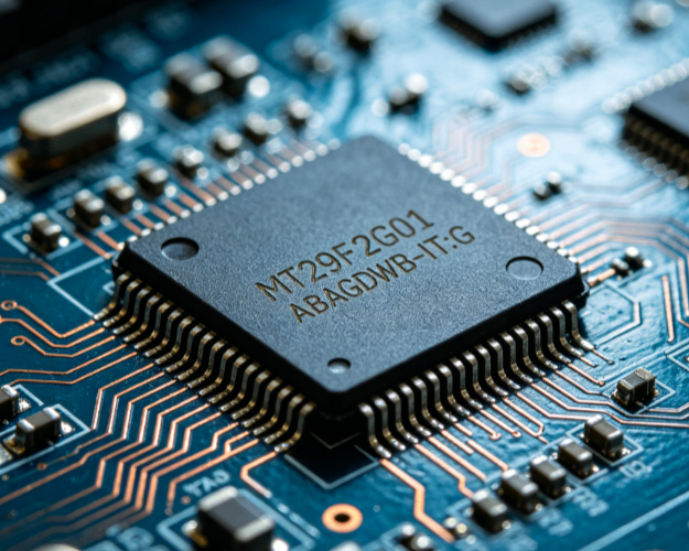
  • MT29F2G01ABAGDWB-IT:G Datasheet: Specs & Performance Guide

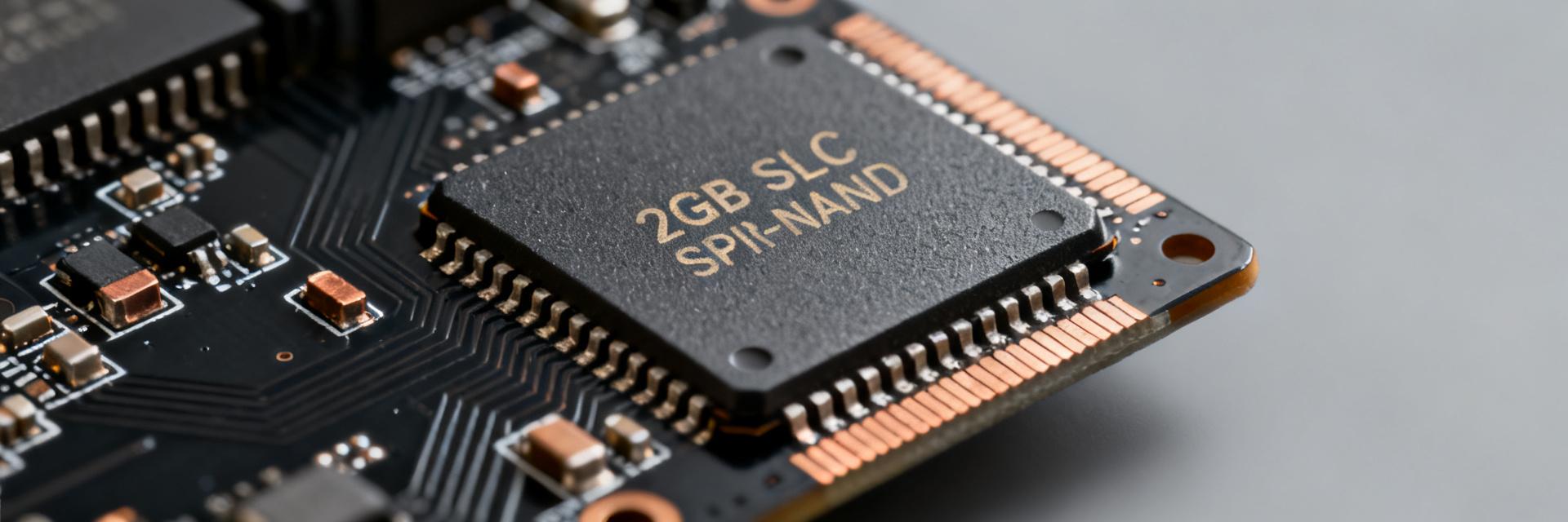
    The MT29F2G01ABAGDWB-IT:G is a 2Gb SLC SPI‑NAND device targeted at reliability‑focused embedded storage. Key metrics — 2Gb density, SLC cell endurance and multi‑I/O SPI throughput — make it a strong candidate for boot, logging and industrial storage. This guide interprets the Datasheet and highlights practical Performance, electrical limits, and design trade‑offs for engineers and procurement specialists. Parameter Specification Notes Density 2Gb (256MB) SLC Technology Interface SPI (x1, x2, x4) Quad I/O Support Voltage (Vcc) 2.7V – 3.6V Standard 3.3V Class Operating Temp -40°C to +85°C Industrial Grade (IT) Page Size 2176 Bytes 2048 + 128 Spare Package 8-pad U-PDFN Compact Footprint 1 — Product overview & key specifications MT29F2G01 SLC NAND CS# CLK SI/SIO0 VCC GND SO/SIO1 1.1 Device identity & memory organization As an SLC 2Gb part, it uses small page/block structures favorable to deterministic writes. A representative page size is ~2176 bytes. Understanding pages/blocks/planes simplifies address mapping, wear distribution, and ECC placement during controller design. 1.2 Electrical & environmental limits The device operates in the 3.3V class with industrial temperature grading. Practical margins include power sequencing, 0.1µF+10µF local decoupling, and layout thermal relief. Add guardbands to current budgets for worst‑case active bursts. 2 — Interface & Performance Analysis 2.1 SPI / x4 I/O Timing The device supports standard SPI and multi‑I/O modes (x1/x2/x4). To estimate practical bandwidth, use: Bandwidth ≈ (clock_rate × data_lines × (useful_bits/total_bits)) × (1 − overhead). Moving to x4 reduces cycles per byte significantly but requires matched routing. 2.2 Endurance & Reliability SLC technology provides superior P/E endurance and retention. However, system ECC and bad‑block management remain essential. Recommended ECC should correct worst-case raw bit error rates (RBER) per product lifetime targets. 3 — Firmware & System Integration Recommended Startup Flow: Power up → Reset → Read ID (0x9F) → Run manufacturer ECC check → Scan blocks for bad-block markers → Build logical-to-physical map → Enable boot operations. 4 — Frequently Asked Questions What is the primary advantage of the MT29F2G01ABAGDWB-IT:G? It offers 2Gb of SLC (Single-Level Cell) NAND which provides superior endurance (typically 100k cycles) and data retention compared to MLC/TLC alternatives, using a simple SPI interface. What are the supported SPI modes for this device? The device supports Standard SPI (x1), Dual SPI (x2), and Quad SPI (x4) modes, significantly increasing read/write throughput during data phases. Does the MT29F2G01ABAGDWB-IT:G require external ECC? While SLC is robust, a minimum of 4-bit or 8-bit ECC is recommended. Many controllers or the on-die ECC engine (if enabled) handle this to ensure data integrity over the device's lifespan. What is the operating temperature range? The 'IT' designation indicates an Industrial Temperature grade, rated for operation from -40°C to +85°C. Summary 2Gb SLC SPI-NAND: Compact form factor, high endurance, and industrial reliability. Design Focus: Power sequencing, matched quad routing, and effective thermal grounding are critical for signal integrity. Firmware Strategy: Implement robust bad-block management and ECC to maximize the 100k P/E cycle potential.
  • MT40A512M16JY-083E: Current Availability & Lifecycle Data

    Recent inventory scans and lifecycle catalogs show increasing listings flagged as limited or obsolete across many DDR4 listings; MT40A512M16JY-083E appears in that same signal set. This brief provides a factual snapshot of availability and lifecycle posture, plus clear substitution guidance for electronics designers and procurement teams. Parameter Specification Details Density 8Gb (512 Meg x 16) Technology DDR4 SDRAM Speed Grade -083E (DDR4-2400) Package FBGA (Fine-pitch Ball Grid Array) Voltage 1.2V (Nominal) 1 — Background: Technical Profile & Roles MT40A512M16JY-083E VDD/VSS Control DQ [0:15] ADDR/BA The MT40A512M16JY-083E is typically used as system DRAM in embedded compute, networking modules, and storage controllers. Designers choose this DDR4 class for its balance of density and power, serving as primary memory or high-throughput buffers in memory-dense subsystems. 2 — Market Availability & Lifecycle Analysis Inventory signals indicate a tightening supply chain. Evidence shows shrinking active listings and rising "limited stock" flags across authorized catalogs. Procurement should interpret "In Stock" signals with caution, as MOQ (Minimum Order Quantity) and lead times are currently volatile. Active/Mature: The part is transitioning from mature to limited support. Warning Signs: Persistent long lead times and datasheet revision changes often precede formal EOL notices. Recommended Cadence: Weekly monitoring of authorized supply channels is advised for active production lines. 3 — Substitution & Risk Mitigation When cross-referencing, the following hierarchy of parameters is mandatory to avoid PCB redesign: Organization & Pinout: Must match 512M x 16 and FBGA ball map exactly. Voltage: 1.2V DDR4 standard is required. Timing: -083E (CL16) or faster can often be used, provided firmware supports the timing tables. Design-for-Supply: Implement flexible footprints and firmware abstraction to allow for multi-sourcing without hardware respins. 4 — Sourcing FAQ Is MT40A512M16JY-083E still in production and available? Availability is currently constrained. Inventory scans indicate limited active listings and emerging obsolete flags. Buyers should request formal lead-time quotes, check authorized supply channels, and plan hedged purchases if immediate production depends on this device. What lifecycle status should I monitor for MT40A512M16JY-083E? Focus on official lifecycle bulletins and datasheet revision logs. Look for removal from mainline catalogs or explicit EOL (End of Life) classifications; those trigger procurement actions such as lifetime buys or engineering redesign. How quickly should I act on limited availability? Act within the window suggested by lead-time trends. If available quantities cover fewer than six months of production, initiate immediate hedged buys and cross-reference evaluations to prevent supply interruptions. What are the critical parameters for a substitute? Essential matches include density (8Gb), organization (x16), bus width, package pinout, and voltage. Mismatching organization or pinout requires a PCB respin, while modest timing differences can often be handled via firmware adjustments.
  • ATMEGA128A-AU Specs & Datasheet: Engineer Quick Ref

    In lab tests and product builds, the ATMEGA128A-AU’s core specs — 128 KB flash, 4 KB SRAM, 4 KB EEPROM, 10-bit ADC and up to 16 MHz clock — determine fit for embedded control and instrumentation. This quick reference aggregates the most used datasheet numbers and actionable design checks. 1 — Quick Specs Summary ParameterValue (typical/limit) Flash Memory128 KB SRAM / EEPROM4 KB / 4 KB Max Clock Speed16 MHz ADC Resolution10-bit, Multiple Channels Operating Voltage2.7V – 5.5V Package Type64-pin TQFP / MLF ATMEGA128A VCC GND UART TX ADC IN RESET 2 — Pinout & Mechanical Details The 64-pin TQFP (10x10mm, 0.8mm pitch) groups VCC/GND banks and dedicated AVCC/AREF pins. When routing, use ferrite beads on the analog supply and place 0.1μF decoupling capacitors within 2–4 mm of each VCC pin to ensure signal integrity. 3 — Electrical Characteristics Expect ~12mA active current at 16MHz/5V (~60mW). Absolute maximum ratings caution against input voltages exceeding VCC±0.5V. Use series resistors for I/O protection and thermal vias under high-load MOSFET switches to manage PCB temperature rise. 4 — Peripherals & Performance CPU: Single-cycle instruction execution for many operations (~16 MIPS). Timers: Multiple counters with PWM for motor/lighting control. Comm: Dual USART, SPI, and TWI (I2C) interfaces. ADC: 8-channel 10-bit converter for sensor integration. 5 — Hardware Integration Checklist Include a 10 kΩ pull-up resistor on the Reset pin. Use 22 pF capacitors for external crystals. Verify ISP (In-System Programming) header pinout for firmware updates. Separate Analog and Digital grounds to minimize ADC noise. 6 — Quick-Reference Troubleshooting UART Communication Failure Check for clock/fuse mismatches. If the internal oscillator is used instead of an external crystal, the baud rate error may exceed acceptable limits. ADC Values are Unstable Verify AREF and AVCC filtering. Ensure the decoupling caps are present and the analog reference voltage is stable. MCU Not Responding via ISP Validate the Reset pull-up and check the SCK frequency of the programmer (must be < 1/4 of the MCU clock). Random Brown-out Resets Confirm the BOD (Brown-Out Detection) fuse levels match your power supply voltage (e.g., 2.7V vs 4.0V). Summary Verify Memory: Confirm 128 KB flash is sufficient for your application code. Power Design: Plan for 2.7–5.5 V operation with adequate decoupling. Prototyping: Use the 64-pin TQFP footprint and include UART/ISP breakouts for early debugging.
  • MT41K256M16TW-107 DDR3L: Performance, Power & Timing Guide

    Point: At 1866 MT/s (933 MHz I/O) and a nominal 1.35V operating voltage, this device yields roughly 3.73 GB/s peak per x16 device—a compact, low-voltage building block for high-speed embedded and networking memory subsystems. Evidence: The throughput calculation (1866 MT/s × 2 bytes) is the datasheet-specified peak. Explanation: This peak is theoretical; system-level overheads will reduce sustained bandwidth, but the device’s profile makes it ideal where board-area and power are constrained. Overview: MT41K256M16TW-107 DDR3L in Context MT41K256M16TW-107 VCC (1.35V) GND DQ [0:15] DQS / CK Quick-spec table ParameterTypical Value Density4 Gb (256M ×16) Max Transfer Rate1866 MT/s Nominal Voltage (Vdd)1.35 V (DDR3L) PackageTFBGA (96-ball) I/O Widthx16 Operating TempCommercial / Industrial Technical Architecture & Organization Internal architecture: prefetch and banks Point: The device uses an internal 8n prefetch with multiple banks that create the observable throughput profile. Evidence: 8n prefetch means each access transfers eight times the core data per clock window. Explanation: Sequential accesses exploiting open rows and bank parallelism yield higher sustained throughput, while random row misses penalize latency. Performance Benchmarks & Methodology Theoretical Peak vs Practical Bandwidth The theoretical peak (≈3.73 GB/s) differs from sustained bandwidth due to controller overhead, refresh cycles, and burst alignment. Designers should expect practical sustained rates to be 70-85% of peak depending on the application's memory access patterns. Power Profile & Thermal Management DDR3L Low-Voltage Behavior Low-voltage operation (1.35V) significantly reduces dynamic power compared to standard 1.5V DDR3. Tip: Measure IDD0, IDD3N, and IDD4R currents under representative workloads to size local VRMs and ensure PDN stability. Timing Parameters & Tuning Signal Integrity Checklist Matched DQ/DQS/CK lengths to within ±5mil for 1866 MT/s. Controlled 40-50 ohm impedance traces for all high-speed signals. Fly-by topology for Address/Command/Control buses. Solid reference plane (GND) directly beneath all memory signal layers. Frequently Asked Questions What are practical sustained bandwidth expectations for x16 DDR3L devices? Sustained bandwidth typically falls below the theoretical peak due to system overhead. Arbitration, refresh, and controller efficiency commonly reduce usable MB/s. Report sequential and random results separately for accurate system modeling. Which currents should I measure to characterize power consumption? Measure active (IDD0), standby (IDD3N), and read/write (IDD4R/W) currents. Include termination currents to build a total power budget and size the VRM and decoupling capacitors appropriately. What layout checks are most likely to improve timing margin? Routing symmetry and controlled impedance are vital. Prioritize matched length for strobes and clocks, add targeted decoupling near power pins, and validate with eye diagrams during controller training. How does 1.35V operation impact the thermal design? While 1.35V operation reduces heat, the high data rate still generates localized thermal load. Ensure thermal vias are placed under the BGA package and verify junction temperature in a thermal chamber.
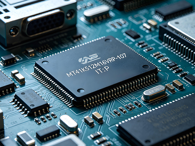
  • 2026 MT41K512M16VRP-107 IT:P In Stock & Price | DDR3L Specs, Lead Time & Replacements

    2026 MT41K512M16VRP-107 IT:P In Stock & Price | DDR3L SDRAM Lead Time, Specs & Alternative Solutions Release Date: May 22, 2026 Abstract The global industrial DDR3L memory market witnesses dynamic supply changes in 2026. Benefiting from adjusted wafer capacity allocation, mainstream industrial memory components see fluctuating delivery cycles and moderate price adjustments. As a high-reliability DDR3L SDRAM product launched by Micron Technology, MT41K512M16VRP-107 IT:P is widely adopted in automotive electronics, industrial control and communication terminal devices. Affected by stock allocation and downstream stocking demand, factory lead time of MT41K512M16VRP-107 IT:P keeps changing, and spot goods become valuable strategic materials for stable production. Our firm releases targeted inventory promotion activities for original genuine MT41K512M16VRP-107 IT:P, supplying sufficient verified in-stock components, favorable 2026 market price and fast cross-border delivery service, effectively helping manufacturers tackle material shortage risks. 1. 2026 Market Lead Time & Supply-Demand Analysis of MT41K512M16VRP-107 IT:P Since the first quarter of 2026, global memory manufacturers have continuously optimized product layout, transferring partial capacity to new-generation DDR5 and LPDDR products, while controlling production volume of mature DDR3L series chips. The market supply of MT41K512M16VRP-107 IT:P presents tight but controllable status. Official factory lead time of MT41K512M16VRP-107 IT:P drops from 12–16 weeks at the beginning of the year to 6–8 weeks in the second quarter. Nevertheless, bulk order delivery may still extend to 10 weeks or above. Driven by stable demand of long-life-cycle industrial and automotive projects, downstream buyers actively reserve stocks, pushing spot quotation of MT41K512M16VRP-107 IT:P to rise slightly. To eliminate production halt hidden dangers caused by insufficient material supply, our company locks abundant original channel inventory of MT41K512M16VRP-107 IT:P via global supply chain cooperation. We launch 2026 limited-time preferential sales policy, providing stable and cost-effective purchasing channels for electronic manufacturing enterprises worldwide. 2. Core Technical Parameters & Industrial Performance of MT41K512M16VRP-107 IT:P MT41K512M16VRP-107 IT:P is an industrial and automotive grade low-voltage DDR3L memory chip, manufactured with mature TwinDie process and compact 96-ball TFBGA package. The component owns outstanding low power consumption, wide temperature adaptability and strong anti-interference capability, and reaches industrial reliability standard with stable operating performance under complex electromagnetic and temperature environments. 2.1 Basic Specifications Part Number: MT41K512M16VRP-107 IT:P Manufacturer: Micron Technology Memory Type: DDR3L SDRAM Storage Density: 8Gb (512M×16 Bit) Max Data Transmission Rate: 1866 MT/s Operating Voltage: 1.283V ~ 1.45V, typical 1.35V Operating Temperature: -40℃ ~ +95℃ industrial wide temperature Package Form: 96-TFBGA Compliance Standard: RoHS lead-free, AEC-Q100 certification 2.2 Key Electrical Indexes Core Supply Voltage: 1.35V low voltage design Maximum Working Current: Standard industrial power consumption level Surge Resistance: Built-in protection circuit, stable voltage bearing capacity Moisture Sensitivity Level: MSL 3, convenient conventional production welding 2.3 Application Advantages Compared with ordinary civil DDR3 memory, MT41K512M16VRP-107 IT:P adapts to harsh working scenes such as vehicle-mounted high temperature and outdoor industrial equipment. Low power design effectively reduces overall device energy consumption, and perfect signal stability ensures long-term uninterrupted operation. For industrial control mainboards, vehicle infotainment and communication control modules, MT41K512M16VRP-107 IT:P is a highly recognized core storage solution. 3. Mainstream Verified Alternative Solutions for MT41K512M16VRP-107 IT:P In view of periodic supply tension and fluctuating lead time of MT41K512M16VRP-107 IT:P, our professional FAE technical team screens and verifies multiple compatible alternative models from pin definition, parameter matching, supply stability and cost performance dimensions, supporting rapid material replacement without PCB and firmware modification. 3.1 Micron Original Pin-to-Pin Replacement MT41K512M16VRN-107 IT:P: Fully consistent package, timing and electrical parameters with MT41K512M16VRP-107 IT:P, zero modification replacement available MT41K512M16VRP-107 AIT:P: Enhanced automotive temperature version, suitable for extreme high and low temperature working projects 3.2 Cross-Brand High Compatibility Alternatives Samsung K4B4G1646E-BYMA: 8Gb DDR3L industrial memory, identical package and compatible performance SK Hynix H5AN8G8NCJR-VKC: Stable supply, matched application scenarios, excellent cost performance 3.3 Selection Guidance Projects requiring original material consistency prefer Micron same-series alternatives; cost-controlled civil and general industrial equipment can choose cross-brand certified DDR3L chips to balance delivery cycle and procurement cost. 4. 2026 Limited Promotion: MT41K512M16VRP-107 IT:P In Stock & Discount Price Aiming at the market procurement shortage of MT41K512M16VRP-107 IT:P, our company rolls out exclusive 2026 stock discount campaign, with sufficient original spot stock and hierarchical bulk preferential prices to satisfy sample test, small batch trial production and mass production demands. 4.1 Inventory & Quality Assurance Total In-stock Quantity: Over 8500 pieces MT41K512M16VRP-107 IT:P Production Batch: Multiple latest batches, original factory sealed packaging Quality Commitment: 100% brand new original parts, support third-party testing, 1-year after-sales warranty 4.2 2026 Tiered Quotation (USD) Small Batch 1-50pcs: $9.10 per unit Medium Batch 51-500pcs: $7.80 per unit Large Batch over 500pcs: $6.60 per unit, super large order negotiable price 4.3 Service Support All in-stock orders can be delivered the next working day, global delivery takes 3-7 working days. Complete datasheets, PCB footprints and one-on-one FAE debugging technical support are provided to accelerate product design and mass production progress. 4.4 Typical Application Scenarios MT41K512M16VRP-107 IT:P is widely applied in industrial PLC control boards, vehicle-mounted multimedia systems, communication base station control units and high-reliability medical embedded equipment. 5. FAQ About MT41K512M16VRP-107 IT:P Purchase & Usage Q1: Are supplied MT41K512M16VRP-107 IT:P genuine new original products? A1: All delivered MT41K512M16VRP-107 IT:P are Micron authentic brand-new components with original sealed package, complete quality traceability and test certification available. Q2: How long is the delivery cycle of in-stock MT41K512M16VRP-107 IT:P order? A2: In-stock goods support immediate shipment, no need to wait 6-8 weeks factory lead time, fast global delivery meets urgent production demands. Q3: Can MT41K512M16VRN-107 IT:P replace MT41K512M16VRP-107 IT:P directly? A3: Yes. Two models share identical package, pin definition and electrical performance, realizing board and program free direct replacement. Q4: How long will the 2026 promotional price of MT41K512M16VRP-107 IT:P stay valid? A4: The preferential activity lasts until June 30, 2026. Price keeps stable during promotion period and will adjust according to market stock status afterward. Q5: Can professional technical support be offered for MT41K512M16VRP-107 IT:P design and debugging? A5: Full set of technical documents and online FAE guidance are provided to help customers finish scheme adaptation and equipment debugging efficiently. Conclusion In 2026, supply fluctuation of mature DDR3L memory will continuously influence embedded and automotive electronic industry. As a classic high-stability storage chip, MT41K512M16VRP-107 IT:P owns irreplaceable application value in long-life-cycle equipment. Our firm supplies abundant original MT41K512M16VRP-107 IT:P in stock and competitive 2026 price, meanwhile offering verified compatible alternatives, helping global purchasers avoid supply chain risks and guarantee steady project progress. Keywords: MT41K512M16VRP-107 IT:P, 2026 In Stock, MT41K512M16VRP-107 IT:P Price, Micron 8Gb DDR3L SDRAM, Industrial Automotive Memory, Embedded Storage Chip