MT40A1G8SA-062E DDR4 - Informe completo de especificaciones y diagrama de pines
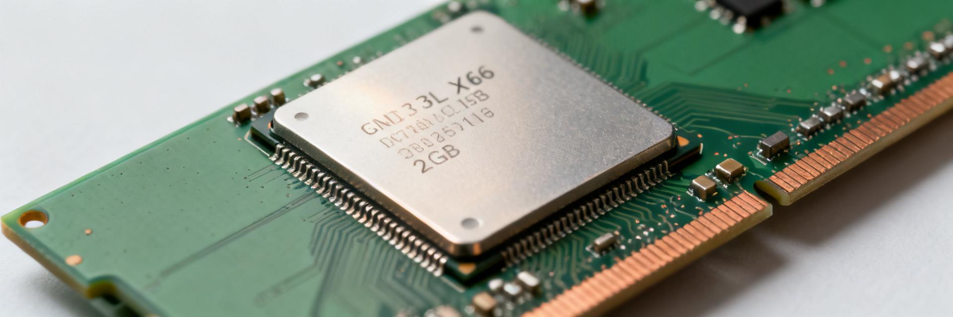
Point: The MT40A1G8SA-062E is an 8 Gbit DDR4 SDRAM organized as 1G x 8 and rated for up to 3200 MT/s with a 1.2 V nominal supply, making it a compact, high-bandwidth die for embedded and board-level memory designs. Evidence: these key values are specified in the device datasheet. Explanation: this report consolidates device specs, pinout, timing, PCB guidance and procurement checks for designers.
Point: Purpose is actionable single-source reference for layout and firmware teams. Evidence: engineers should cross-check every numeric limit against the vendor DDR4 datasheet (device revision) during design sign-off. Explanation: use the pinout table and timing summaries below as starting inputs for PHY settings, SI simulations, and procurement verification.
1 → Overview & Key Specifications (background)
Part organization & capacity
Point: Organization string is explicitly given as 1G x 8 for the device, yielding an 8 Gbit density. Evidence: the datasheet organization field reads "1G x 8" for the packaged die. Explanation: that organization implies an 8-bit wide data bus per chip; designers must map device density into controller address/row/col calculations when populating ranks and channels.
Electrical summary & supported speeds
Point: Nominal VDD / VDDQ is 1.2 V and the device supports speed grades up to 3200 MT/s. Evidence: the speed/grade table in the DDR4 datasheet lists 3200 MT/s as the upper supported transfer rate and specifies typical CAS latency ranges. Explanation: target timing and thermal budgets around 1.2 V operation and verify CL/tCK combinations from the datasheet for chosen speed grade.
2 → Electrical Characteristics & Timing Parameters (data analysis)
DC characteristics & power
Point: Verify Vmin/Vmax, Idd standby/active, and VREF requirements directly from the datasheet. Evidence: the datasheet lists nominal VDD = 1.2 V and a VREF ≈ VDD/2; device tables provide Idd ranges for standby and active modes. Explanation: plan local decoupling near VDD/VDDQ balls, follow recommended VREF decoupling, and flag any outlying DC limits for power budgeting before prototype.
AC timing & performance parameters
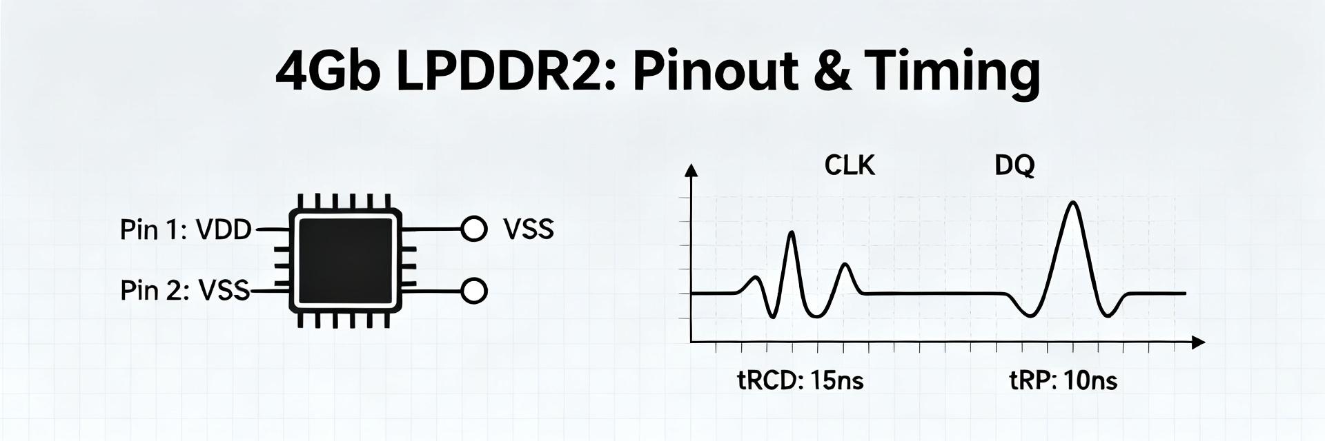
Point: Key timing parameters to extract include tCK, CL, tRCD, tRP, tRAS, tRFC, tFAW, tWR and tWTR. Evidence: at 3200 MT/s tCK ≈ 0.625 ns; CAS latency at this rate commonly ranges in JEDEC grades (see datasheet tables). Explanation: use the datasheet timing table to populate PHY timing registers and validate with a timing table in SI tools.
| Parameter | Example @3200 MT/s | Reference JEDEC Standard |
|---|---|---|
| tCK (Clock Cycle Time) | ≈ 0.625 ns | DDR4-3200 (CL = 22) |
| CAS Latency (CL) | Typical range (22-22-22) | See Vendor Datasheet Table |
| tRCD / tRP | Configured per JEDEC/speed grade | 13.75 ns (nominal) |
| tRFC (Refresh Cycle Time) | 350 ns (8 Gbit density) | Standard refresh recovery boundary |
3 → Pinout, Package & Mechanical Details (data analysis)
Pinout map & signal grouping
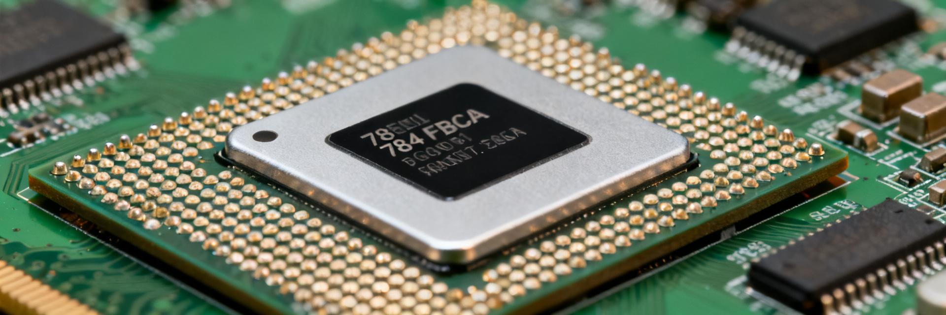
Point: The device uses a 78-ball FBGA with grouped signals: DQ, DQS/DM, CK/CK#, CA/address & command, BA, CKE, ODT, VSS, VDD and NC. Evidence: the package pinmap table in the datasheet enumerates each ball ID and net name for quick cross-reference. Explanation: include an annotated pinout CSV for the placement team and ensure DQS/DQ grouping matches controller lane assignments during layout.
Package dimensions, land pattern & thermal notes
Point: Follow mechanical drawing for FBGA dimensions, land pattern, and thermal via recommendations. Evidence: the mechanical section gives package X×Y size, ball pitch, and recommended PCB land pattern tolerances. Explanation: design thermal vias under the exposed copper area per drawing, respect height constraints for z-stack, and verify pick-and-place clearances with the assembler.
4 → PCB Routing & Signal-Integrity Best Practices (method guide)
Routing, termination & impedance control
Point: Maintain controlled impedance and aggressive length matching for DQ/DQS and CK nets. Evidence: recommended targets are roughly 40–60 Ω single-ended for DQ and matched DQ-to-DQS group lengths; minimize stubs and follow ODT guidance. Explanation: use differential pairs for CK/CK# where applicable, match DQS capture timing to DQ within specified ppm, and validate with SI simulations before tape-out.
Power distribution & decoupling strategy
Point: PDN must place local decoupling near VDD/VDDQ balls with layered cap networks. Evidence: datasheet and PDN best practices call for combinations of 0.01–0.1 µF (high-frequency) and 4.7–47 µF (bulk) caps close to device power pins and VREF caps. Explanation: place decouplers within 2–4 mm of power pins, route wide copper planes, and verify with PDN impedance sweeps aligned to switching frequencies.
5 → Integration Checklist: Firmware, PHY Training & Validation (method/case)
PHY/Controller settings & training sequence
Point: Document PHY registers for timing, ODT, drive strength, and VREF calibration as starting points. Evidence: typical training includes CK calibration, read/write leveling, and DQ/DQS alignment; example register presets exist in PHY vendor guides (use as starting point). Explanation: treat example values as provisional—confirm exact register values against the datasheet and PHY vendor recommendations during bring-up.
Validation tests & acceptance criteria
Point: Prioritize JEDEC compliance, read/write sweeps, BERT, eye-diagram margins, thermal cycling and retention checks. Evidence: acceptance criteria should be based on datasheet timing margins and SI eye targets; require zero uncorrected ECC errors over test windows. Explanation: run automated test sequences across PVT corners, log margin shifts, and require stated timing guard-bands before sign-off.
6 → Procurement, Part Variants & Compliance Checks (action advice)
Identifying suffixes, lifecycle & cross-references
Point: Decode suffixes for speed, temperature grade and packaging when ordering. Evidence: part marking and ordering codes in the datasheet identify package, speed grade and temperature range—verify against the BOM. Explanation: confirm footprint and pin compatibility before substituting cross-references and request revision-level datasheets from the vendor for traceability.
Compliance, RoHS & obsolescence checks
Point: Confirm RoHS/REACH declarations, JEDEC compliance level and active lifecycle status before procurement. Evidence: datasheet or vendor documentation indicates compliance and revision notes; distributors can provide traceability documents. Explanation: request certificate of compliance and latest datasheet revision when qualifying suppliers to avoid obsolescence or non-compliant inventory.
Conclusion
Point: The MT40A1G8SA-062E is an 8 Gbit DDR4 device (1Gx8) supporting up to 3200 MT/s at 1.2 V with a 78-ball FBGA pinout. Evidence: key specs and pin assignments are listed in the device datasheet and pinout tables. Explanation: designers should treat the DDR4 datasheet and the pinout table above as the authoritative references for layout, PHY configuration, and procurement.
Key Summary
- Device: MT40A1G8SA-062E — 8 Gbit, organization 1G x 8; use datasheet organization string to map memory addressing and ranks precisely.
- Electrical & timing: Nominal VDD/VDDQ = 1.2 V; target up to 3200 MT/s; extract tCK, CL, tRCD, tRP, tRFC from the DDR4 datasheet tables for PHY setup.
- Layout & validation: 78-ball FBGA pinout requires grouped DQ/DQS routing, controlled impedance, local decoupling, and full PHY training plus JEDEC-style validation tests.
Frequently Asked Questions
What is the MT40A1G8SA-062E organization and capacity?
Answer: The device is organized as 1G x 8 producing an 8 Gbit density. Use the organization string from the datasheet to compute rank, column and row address mapping and to determine how many devices are required per rank for your target bus width.
Which timing parameters must I load into the PHY for 3200 MT/s?
Answer: Populate tCK, CAS (CL), tRCD, tRP, tRAS, tRFC, tFAW, tWR and tWTR from the datasheet’s speed-grade timing table. Start with PHY vendor example registers, then refine during training using observed timing margins from eye-diagrams and BER testing.
What PCB practices ensure signal integrity for this 78-ball FBGA?
Answer: Maintain 40–60 Ω single-ended impedance for DQ, tightly length-match DQ to associated DQS within group budgets, minimize stubs, place terminations or rely on ODT per datasheet guidance, and deploy local decoupling caps near VDD/VDDQ balls; verify with SI and PDN simulations.
What are the nominal power supply requirements and decoupling recommendations?
Answer: The nominal operational voltage is VDD = VDDQ = 1.2V, with VPP specified at 2.5V. Decoupling requires a localized matrix of high-frequency MLCC capacitors (0.01µF to 0.1µF) placed inside a 2-4mm radius of the VDD/VDDQ power pins, bolstered by 4.7µF to 47µF bulk capacitors.