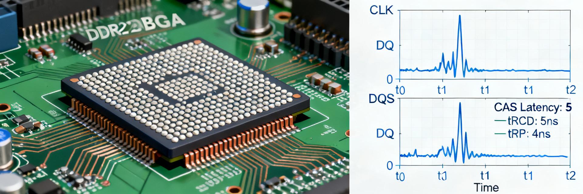
LPDDR3 NT6CL512F32BM-H3: Отчет о емкости и тестировании
This report summarizes targeted lab objectives and what engineers will take away: a reproducible benchmark methodology, capacity interpretation for the NT6CL512F32BM-H3 part, and practical performance expectations for mobile/embedded classes where LPDDR3 remains relevant. Readers will see how measured throughput bands, latency profiles, and power‑efficiency tradeoffs map to design choices and validation checkpoints.
Test objectives: establish sustained and peak throughput envelopes, quantify random vs. sequential latency behavior, and characterize power/thermal envelopes under sustained load. The intent is practical guidance: how to confirm datasheet fields, run a repeatable benchmark, and interpret results for system selection.
1 — Overview & Key Specifications (background)
1.1 — Module identity & capacity breakdown
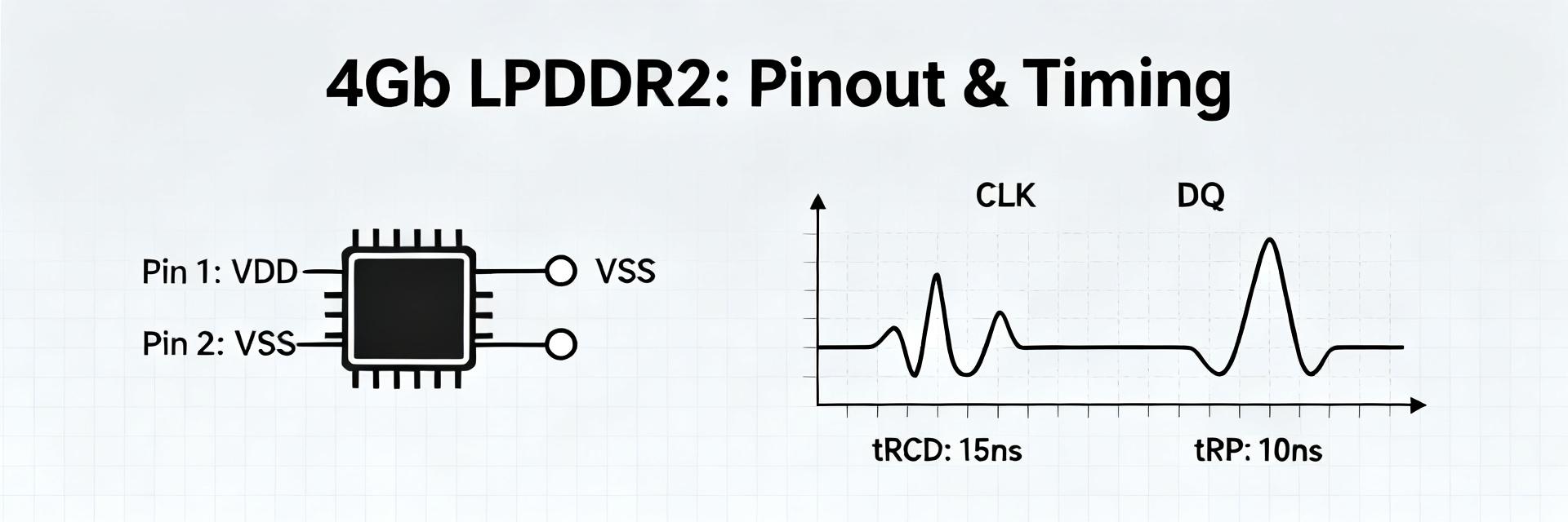
Report the following fields for NT6CL512F32BM-H3: package type (PoP/FBGA), nominal die density (Gb per die), die count per package, bus width per die (x4/x8/x16), total module capacity (GiB), nominal I/O voltage, and JEDEC timing grade. Actionable checklist items: confirm top‑side markings, package code, datasheet part number, density codes, and any rank/stack indicators. Note LPDDR3 signaling and low‑voltage rails when recording power rails.
1.2 — Where LPDDR3 fits vs. other mobile DRAM generations
LPDDR3 targets mid‑tier mobile and embedded systems where moderate bandwidth and low standby power are priorities. It trades lower peak bandwidth versus newer LPDDR generations for simpler controller logic and mature power profiles. Typical module sizes top out in single‑digit gigabytes per device in common system configurations; larger capacities require multiple devices or stacked packages and may hit controller addressing limits.
2 — Benchmark Methodology & Test Setup (method guide)
2.1 — Hardware and software test rig (reproducibility checklist)
Specify memory controller model and firmware revision, board schematic notes (trace lengths, termination), reference clock, and I/O width used. Use OS/kernel versions and benchmark tool versions in logs. Recommended benchmark tools: stream-style throughput tester, randomized traffic generator, latency microbenchmarks, and precision power meters. Include a reproducibility checklist: target clock rates, I/O width, temperature, test patterns, and number of runs. Label each log with config and timestamp.
- Checklist template: clock rates, I/O width, VDD/VDDQ rails, ambient temp, trace length notes.
- Log entries to record: controller settings, refresh policy, benchmark seed, sample index.
2.2 — Test scenarios and metrics
Measure sustained bandwidth (MB/s), peak instantaneous bandwidth, sequential/read/write mixes, random 4K/64K latency (ns), page‑open/page‑close behavior, idle vs. active power, and temperature rise under load. Recommended runtimes: 60–300s per scenario to reach steady state; at least 5 independent runs for statistics. Report mean and standard deviation and flag outliers for investigation.
3 — Capacity Analysis & Raw-Spec Interpretation (data analysis)
3.1 — Effective usable capacity and addressing constraints
Translate die density and x‑width into usable module capacity with this formula: Module GB = (die Gb × die count × bits per die) / 8 / 1024. Confirm any address multiplexing or bank‑count limits that reduce usable range. For NT6CL512F32BM-H3, verify die count and bus configuration on the package marking to avoid overstating usable system RAM when multiple devices share a channel.
3.2 — Timing parameters, frequency bands, and expected peak throughput
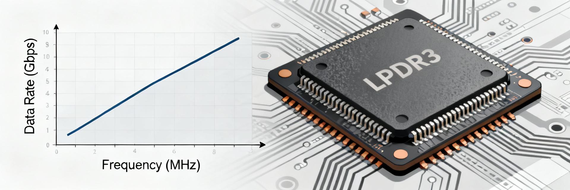
Use timing numbers (tCK, CL, tRCD, tRP) and effective data rate (MT/s) to compute theoretical throughput: Theoretical BW = (DataRate MT/s × bus width bits) / 8. Expect measured throughput below theory due to controller overhead, refresh, and bank conflicts. Provide a table mapping common clock points to theoretical and realistic ranges for easy comparison.
| Clock (MHz) | Data Rate (MT/s) | Theoretical BW (MB/s) | Expected Measured Range (MB/s) |
|---|---|---|---|
| 800 MHz | 1600 MT/s | 6,400 MB/s (x32 Interface) | 5,120 – 5,760 MB/s (80% - 90% efficiency) |
| 933 MHz | 1866 MT/s | 7,464 MB/s (x32 Interface) | 5,970 – 6,710 MB/s (80% - 90% efficiency) |
4 — Benchmark Results & Comparative Performance (data analysis)
4.1 — Measured throughput & latency results (read/write, mixed)
Present sequential read/write, random read/write, and mixed workload results as annotated charts or tables. For each workload include sample mean, std dev, and run count. Annotate anomalies such as controller throttling, refresh spikes, or thermal slope effects. When discussing LPDDR3 results, call out controller settings that produced best sustained throughput and any tradeoffs that reduced latency at the expense of bandwidth.
4.2 — Power, thermal behavior, and efficiency (GB/s per watt)
Report idle and active power with precision meters and plot power vs. throughput. Compute an efficiency metric (MB/s per watt) and normalize for board differences by reporting per‑module and per‑system metrics. Include temperature rise over baseline after sustained runs and identify any thermal throttling points. Where possible, provide normalized curves rather than single snapshot numbers.
5 — Real-world Use Cases, Comparative Notes & Recommendations (case + action)
5.1 — Best-fit application scenarios and trade-offs
Map observed throughput, latency, and power to target applications. The NT6CL512F32BM-H3 suits mid‑tier mobile and embedded vision tasks that require modest sustained bandwidth with constrained thermal envelopes. It is less appropriate for high‑bandwidth AI accelerators or memory‑bound server workloads. Use a short selection checklist: required capacity, peak bandwidth threshold, and thermal budget to decide fit.
5.2 — Integration guidance & test-before-deploy checklist
Integration steps: verify VDD rails and decoupling, confirm signal‑integrity on critical traces, and lock controller timing to datasheet margins. Must‑test validations: long‑duration throughput run, randomized latency under mixed traffic, power profiling under target load, and thermal soak at expected enclosure conditions. Record firmware/controller settings used for any passing validation.
Conclusion (summary + next steps)
LPDDR3 remains a pragmatic choice where mature controller ecosystems, modest bandwidth, and constrained thermal envelopes align with system requirements. For the NT6CL512F32BM-H3, designers should validate capacity mapping, run the provided benchmark checklist, and confirm thermal behavior in the actual enclosure. Next steps: execute the reproducibility checklist, normalize power measurements, and select capacity based on observed workload patterns.
Key Summary
- Confirm package fields and die configuration for NT6CL512F32BM-H3 to derive usable GB; record package markings and bus width to avoid addressing surprises in system builds.
- Use the provided benchmark checklist and run multiple long‑duration scenarios to capture steady‑state throughput, latency distributions, and thermal trends for LPDDR3 modules.
- Normalize power vs. throughput to compute MB/s per watt and apply the selection checklist: required capacity, sustained bandwidth threshold, and thermal envelope before deployment.
Frequently Asked Questions
How does NT6CL512F32BM-capacity per package translate to system memory?
Convert die density and counts using: Total bytes = (Gb per die × die count) / 8. Then account for bus width and any interleaving or rank limitations imposed by the controller. Always confirm markings and datasheet density codes to avoid overstatement of usable system memory.
What are the most important LPDDR3 benchmark metrics to report?
Report sustained and peak bandwidth (MB/s), random and sequential latency (ns), idle and active power (W), and thermal rise under sustained load. Include mean and standard deviation across multiple runs and annotate any controller or thermal throttling observed during measurements.
Which pre‑deployment tests are must‑run for integration?
Run a long‑duration sustained throughput test, randomized latency under mixed traffic, power profiling under expected duty cycles, and a thermal soak in the target enclosure. Verify controller timing margins and confirm that power rails and decoupling meet datasheet recommendations before production release.
What are the exact power rails and critical operating values for NT6CL512F32BM-H3?
This LPDDR3 SDRAM utilizes low-voltage rails consisting of VDD1 (core power) at 1.8V nominal, VDD2 (peripheral circuit) at 1.2V nominal, and VDDQ (I/O interface) at 1.2V nominal. Keeping these lines stabilized using proper bulk and bypass decoupling capacitors is necessary to avoid signal integrity breakdown during fast transition states.