NT5TU32M16FG-AC DDR2 512Mb: Полные спецификации и метрики
TL;DR: A single-rank, x16 DDR2 device built for legacy embedded systems offering 512Mb density; confirm electrical and timing values from the datasheet before integration. This page provides a concise, actionable reference covering NT5TU32M16FG-AC and DDR2 512Mb specs, package guidance, performance expectations, integration checklist and lifecycle actions for system designers.
Many legacy embedded boards still rely on DDR2-class memory, so a precise component sheet matters for validation and sourcing. Evidence shows that NT5TU32M16FG-AC and DDR2 512Mb devices remain common in industrial and low-cost designs. Accurate part identification and verification reduce design re-spins and procurement risk; this article aims to deliver a single-page actionable reference for designers.
1 — Product overview & key identifiers
— What NT5TU32M16FG-AC refers to
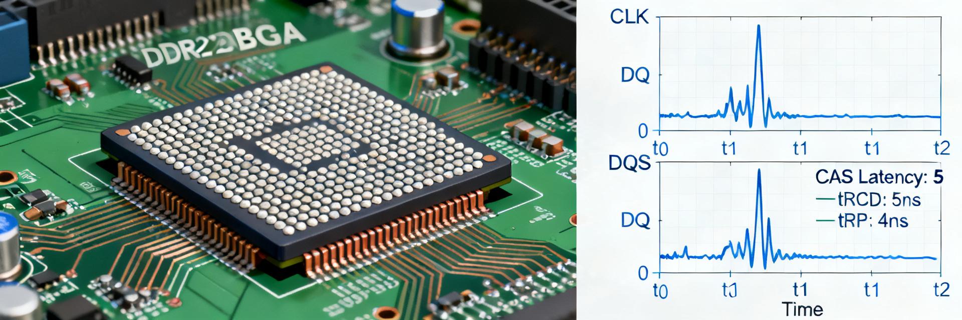
The part string encodes density, organization and family. The marking denotes a 512Mb device organized as 32M x16, and the suffix indicates package/grade specifics. Designers should read the full part marking and package code in the datasheet to confirm BGA-style package family, ballout variant and any tape-and-reel versus tray options before placing the part on a BOM.
— Typical use cases & compatibility notes
DDR2 512Mb x16 devices are widely used in legacy embedded platforms and simple consumer boards. Typical systems include industrial controllers, legacy networking gear and low-cost multimedia boards that require moderate memory bandwidth. Compatibility checks must include controller pincount, voltage domain alignment (VDD/VDDQ), address mapping and rank/chip-select support to ensure firmware and memory controller training succeed.
2 — Electrical characteristics & supply requirements
— Core electrical parameters
Key electrical items to capture are nominal voltages, operating currents and I/O levels. For DDR2-class devices the nominal VDD/VDDQ is 1.8V. Standby, active, read/write, and listed power-saving modes must be evaluated with typical vs max conditions. Designers should copy exact numeric IDD entries from the datasheet, verifying parameters at specific temperature ranges and speed grades.
| Parameter | Specs & Value Limits | Test Conditions / Notes |
|---|---|---|
| Density & Organization | 512 Megabit / 32M x 16 | Single-Rank Architecture |
| Supply Voltage (VDD/VDDQ) | 1.8V ± 0.1V | Nominal operating range |
| Speed / CAS Latency | DDR2-800 @ CL5 / CL6 | tCK = 2.5ns (CL=5) |
| Active / Standby Current | IDD0 / IDD2P / IDD3N | Refer to Nanya datasheet specifications |
| Package Specification | 84-ball WBGA (8mm x 12.5mm) | Halogen-Free, Lead-Free, RoHS compliant |
| Operating Temperature | 0°C to +85°C (Commercial) | TC (Case Temperature) limits apply |
— Timing & signaling
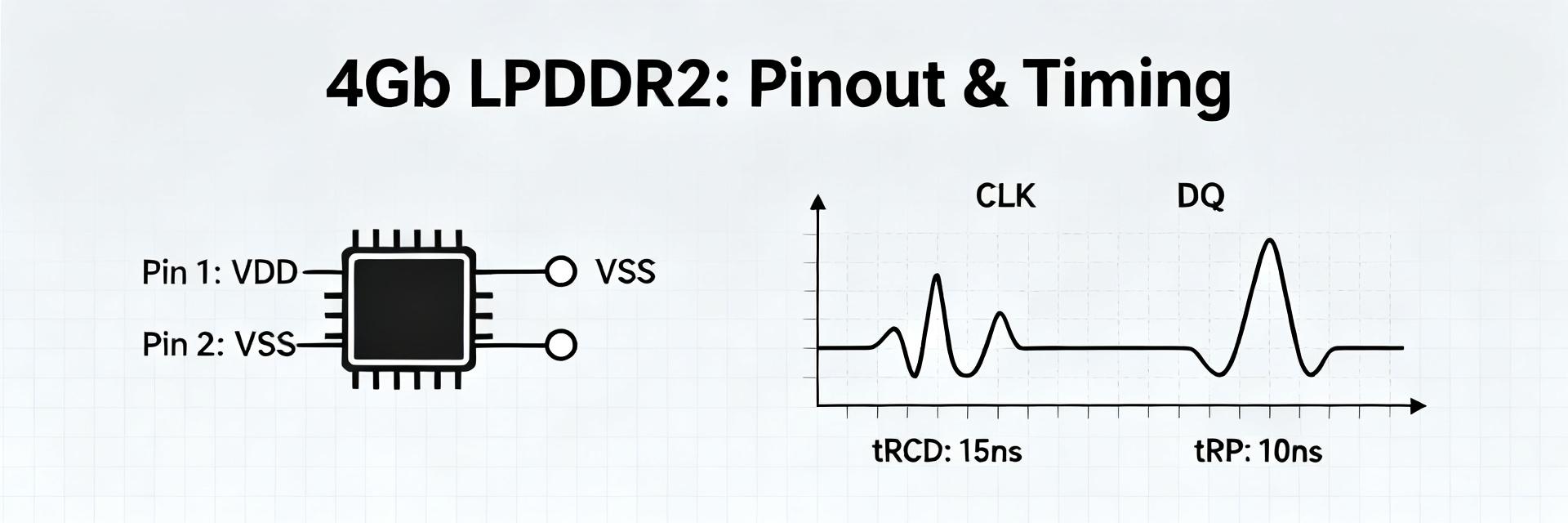
Timing parameters determine usable latency and controller configuration. The datasheet reports critical parameters such as tRCD, tRP, tRAS, CAS latency options, burst length, and maximum supported data rate. Use the timing table to derive access time:
Access = (CL × tCK) + command overhead
Prioritize worst-case timing values for system timing budgets and signal integrity planning.
3 — Physical, packaging & mechanical metrics
— Package, pinout & footprint guidance
Package details directly affect PCB layout and assembly. Record BGA ball count, ball pitch, and package dimensions as published in the mechanical drawing. Ensure footprint tolerances match the supplier drawing, check recommended land pattern, and validate solder paste stencil openings before first PCB spin.
— Thermal & reliability ratings
Thermal and reliability data determine application suitability. Capture operating temperature ranges (commercial vs industrial), thermal resistance (θJA/θJC), RoHS/lead-free statements and any MTBF ratings. Apply thermal mitigation such as solid ground planes, thermal vias under the BGA package, and clean decoupling topology to ensure system reliability under full operational loads.
4 — Performance benchmarks & system-level metrics
— Throughput, latency and real-world expectations
Translate device parameters into system bandwidth and access times for practical design trade-offs. For a single-rank x16 DDR2 device operating at DDR2-800, the theoretical maximum bandwidth is approximately 1.6 GB/s. Random-access latency is defined by structural parameters like CAS Latency (CL), Row Active Time (tRAS), and Cycle Time (tCK), where actual timing is optimized through memory controller registers.
— Power vs performance trade-offs
Power scales with frequency and active cycles. Typical DDR2 power rises with higher clock rates and with more frequent refresh/read-write activity; standby modes reduce current substantially. Compare speed grades by measuring IDD active at rated speed, then select the slower grade for power-constrained designs or the faster grade when throughput is the priority; always verify with datasheet IDD numbers.
5 — Integration checklist: PCB layout, signal integrity & BOM
— PCB layout and routing best practices
Layout governs signal integrity and reliable DDR2 operation. Designers must follow strict layout guidelines:
- Execute tight length matching within DQ and DQS strobe groups.
- Provide clean reference ground planes without stitching cuts under memory signals.
- Place decoupling capacitors directly adjacent to the corresponding VDD/VDDQ balls.
- Keep trace impedance matched to 50 ohms single-ended and 100 ohms differential.
— BOM & procurement notes
Procurement must confirm variant, speed and thermal grade to avoid mismatches. Verify package variant (tray vs tape & reel), speed-grade marking, temperature grade and full part marking against the datasheet. Record supplier documentation and datasheet revision on the BOM, request sample quantities for initial validation and maintain a validated alternate part family to mitigate availability risks.
6 — Validation, testing & lifecycle considerations
— Functional test & verification procedures
A concise test plan catches integration defects early. Key validation procedures include:
- Verify initial power-up rails (VDD and VDDQ sequencing).
- Run controller calibration loops (Read/Write margin training).
- Execute diagnostic memory patterns (Walking-bits, stress test blocks).
- Run long-term burn-in tests at high operating temperature to confirm stability.
— End-of-life, replacements & design-for-obsolescence
Prepare for EOL by validating alternates and cross-referencing markings. Identify superseded speed grades and confirm drop-in replacements by timing, VDD and ballout compatibility. Maintain a qualified alternate part family, version-control the BOM, and use firmware configurability to accommodate minor timing differences as short-term mitigation when direct drop-in options are unavailable.
Summary
- NT5TU32M16FG-AC occupies the DDR2 512Mb x16 class; confirm the device family and package drawing against your BOM and controller requirements to avoid integration mismatches.
- Key specs to verify in the datasheet are VDD/VDDQ (nominal 1.8V), IDD values (standby/active/read/write), timing entries (tRCD, tRP, tRAS, CL) and package dimensions for correct footprint.
- Critical integration actions include matched-length routing for DQ/DQS groups, tight decoupling, thermal mitigation for the BGA package and a validated alternate part to address obsolescence; consult the datasheet for final specs.
Frequently Asked Questions
What are the essential NT5TU32M16FG-AC DDR2 512Mb specs to confirm before layout?
Confirm nominal VDD/VDDQ (1.8V), IDD operating and standby currents with specified conditions, CAS latency options and supported data rate, BGA package dimensions and exact ballout. Verify timing tables for worst-case values and ensure the board footprint matches the supplier mechanical drawing before first assembly.
How should a designer validate NT5TU32M16FG-AC memory timing during bring-up?
Run controller initialization and training sequences, exercise JEDEC timing verification patterns, and use walking-bit and sustained burst tests to validate density and data integrity. Record training tables from the controller and compare against datasheet timing margins; thermal soak under load confirms stability across operating temperatures.
What steps reduce risk of obsolescence for DDR2 512Mb parts?
Maintain a qualified set of alternate parts with compatible ballout and timing, track datasheet revisions and supplier notifications, and version-control BOMs. Where available, validate firmware timing configurability to accept small timing deltas and plan for stocking critical quantities during transitions.
How to handle DDR2 signal integrity and termination (ODT) for NT5TU32M16FG-AC?
Ensure proper layout termination by enabling internal On-Die Termination (ODT) parameters in the controller and the DDR2 register settings (75, 150, or 50-ohm depending on topology). Follow length-matching routing rules for DQ/DQS strobe groups and maintain continuous references planes to prevent impedance discontinuities.