• MT40A1G8SA-062E DDR4 - Полный спецификации и схема выводов

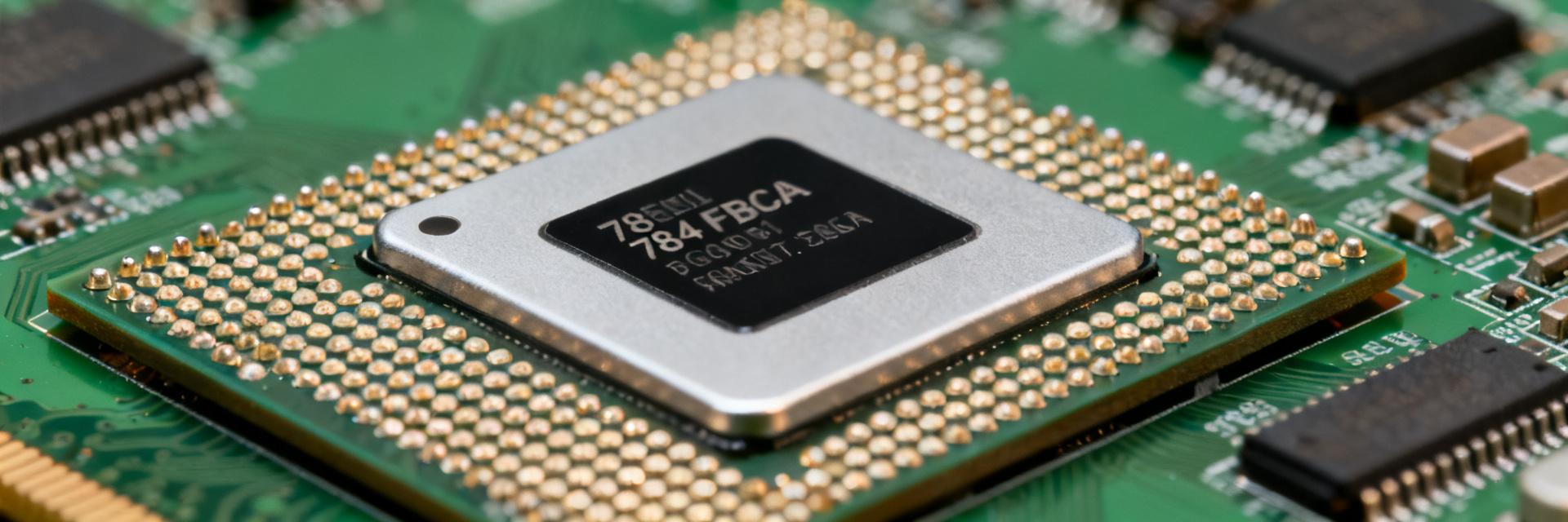
    Point: The MT40A1G8SA-062E is an 8 Gbit DDR4 SDRAM organized as 1G x 8 and rated for up to 3200 MT/s with a 1.2 V nominal supply, making it a compact, high-bandwidth die for embedded and board-level memory designs. Evidence: these key values are specified in the device datasheet. Explanation: this report consolidates device specs, pinout, timing, PCB guidance and procurement checks for designers. Point: Purpose is actionable single-source reference for layout and firmware teams. Evidence: engineers should cross-check every numeric limit against the vendor DDR4 datasheet (device revision) during design sign-off. Explanation: use the pinout table and timing summaries below as starting inputs for PHY settings, SI simulations, and procurement verification. 1 → Overview & Key Specifications (background) Part organization & capacity Point: Organization string is explicitly given as 1G x 8 for the device, yielding an 8 Gbit density. Evidence: the datasheet organization field reads "1G x 8" for the packaged die. Explanation: that organization implies an 8-bit wide data bus per chip; designers must map device density into controller address/row/col calculations when populating ranks and channels. Electrical summary & supported speeds Point: Nominal VDD / VDDQ is 1.2 V and the device supports speed grades up to 3200 MT/s. Evidence: the speed/grade table in the DDR4 datasheet lists 3200 MT/s as the upper supported transfer rate and specifies typical CAS latency ranges. Explanation: target timing and thermal budgets around 1.2 V operation and verify CL/tCK combinations from the datasheet for chosen speed grade. MT40A1G8SA-062E 8 Gbit DDR4 • 1G x 8 CK / CK# A[14:0] / BG[1:0] CKE / ODT / CS# DQ[7:0] DQS_t / DQS_c VDD / VDDQ (1.2V) 2 → Electrical Characteristics & Timing Parameters (data analysis) DC characteristics & power Point: Verify Vmin/Vmax, Idd standby/active, and VREF requirements directly from the datasheet. Evidence: the datasheet lists nominal VDD = 1.2 V and a VREF ≈ VDD/2; device tables provide Idd ranges for standby and active modes. Explanation: plan local decoupling near VDD/VDDQ balls, follow recommended VREF decoupling, and flag any outlying DC limits for power budgeting before prototype. AC timing & performance parameters Point: Key timing parameters to extract include tCK, CL, tRCD, tRP, tRAS, tRFC, tFAW, tWR and tWTR. Evidence: at 3200 MT/s tCK ≈ 0.625 ns; CAS latency at this rate commonly ranges in JEDEC grades (see datasheet tables). Explanation: use the datasheet timing table to populate PHY timing registers and validate with a timing table in SI tools. Parameter Example @3200 MT/s Reference JEDEC Standard tCK (Clock Cycle Time) ≈ 0.625 ns DDR4-3200 (CL = 22) CAS Latency (CL) Typical range (22-22-22) See Vendor Datasheet Table tRCD / tRP Configured per JEDEC/speed grade 13.75 ns (nominal) tRFC (Refresh Cycle Time) 350 ns (8 Gbit density) Standard refresh recovery boundary 3 → Pinout, Package & Mechanical Details (data analysis) Pinout map & signal grouping Point: The device uses a 78-ball FBGA with grouped signals: DQ, DQS/DM, CK/CK#, CA/address & command, BA, CKE, ODT, VSS, VDD and NC. Evidence: the package pinmap table in the datasheet enumerates each ball ID and net name for quick cross-reference. Explanation: include an annotated pinout CSV for the placement team and ensure DQS/DQ grouping matches controller lane assignments during layout. Package dimensions, land pattern & thermal notes Point: Follow mechanical drawing for FBGA dimensions, land pattern, and thermal via recommendations. Evidence: the mechanical section gives package X×Y size, ball pitch, and recommended PCB land pattern tolerances. Explanation: design thermal vias under the exposed copper area per drawing, respect height constraints for z-stack, and verify pick-and-place clearances with the assembler. 4 → PCB Routing & Signal-Integrity Best Practices (method guide) Routing, termination & impedance control Point: Maintain controlled impedance and aggressive length matching for DQ/DQS and CK nets. Evidence: recommended targets are roughly 40–60 Ω single-ended for DQ and matched DQ-to-DQS group lengths; minimize stubs and follow ODT guidance. Explanation: use differential pairs for CK/CK# where applicable, match DQS capture timing to DQ within specified ppm, and validate with SI simulations before tape-out. Power distribution & decoupling strategy Point: PDN must place local decoupling near VDD/VDDQ balls with layered cap networks. Evidence: datasheet and PDN best practices call for combinations of 0.01–0.1 µF (high-frequency) and 4.7–47 µF (bulk) caps close to device power pins and VREF caps. Explanation: place decouplers within 2–4 mm of power pins, route wide copper planes, and verify with PDN impedance sweeps aligned to switching frequencies. 5 → Integration Checklist: Firmware, PHY Training & Validation (method/case) PHY/Controller settings & training sequence Point: Document PHY registers for timing, ODT, drive strength, and VREF calibration as starting points. Evidence: typical training includes CK calibration, read/write leveling, and DQ/DQS alignment; example register presets exist in PHY vendor guides (use as starting point). Explanation: treat example values as provisional—confirm exact register values against the datasheet and PHY vendor recommendations during bring-up. Validation tests & acceptance criteria Point: Prioritize JEDEC compliance, read/write sweeps, BERT, eye-diagram margins, thermal cycling and retention checks. Evidence: acceptance criteria should be based on datasheet timing margins and SI eye targets; require zero uncorrected ECC errors over test windows. Explanation: run automated test sequences across PVT corners, log margin shifts, and require stated timing guard-bands before sign-off. 6 → Procurement, Part Variants & Compliance Checks (action advice) Identifying suffixes, lifecycle & cross-references Point: Decode suffixes for speed, temperature grade and packaging when ordering. Evidence: part marking and ordering codes in the datasheet identify package, speed grade and temperature range—verify against the BOM. Explanation: confirm footprint and pin compatibility before substituting cross-references and request revision-level datasheets from the vendor for traceability. Compliance, RoHS & obsolescence checks Point: Confirm RoHS/REACH declarations, JEDEC compliance level and active lifecycle status before procurement. Evidence: datasheet or vendor documentation indicates compliance and revision notes; distributors can provide traceability documents. Explanation: request certificate of compliance and latest datasheet revision when qualifying suppliers to avoid obsolescence or non-compliant inventory. Conclusion Point: The MT40A1G8SA-062E is an 8 Gbit DDR4 device (1Gx8) supporting up to 3200 MT/s at 1.2 V with a 78-ball FBGA pinout. Evidence: key specs and pin assignments are listed in the device datasheet and pinout tables. Explanation: designers should treat the DDR4 datasheet and the pinout table above as the authoritative references for layout, PHY configuration, and procurement. Key Summary Device: MT40A1G8SA-062E — 8 Gbit, organization 1G x 8; use datasheet organization string to map memory addressing and ranks precisely. Electrical & timing: Nominal VDD/VDDQ = 1.2 V; target up to 3200 MT/s; extract tCK, CL, tRCD, tRP, tRFC from the DDR4 datasheet tables for PHY setup. Layout & validation: 78-ball FBGA pinout requires grouped DQ/DQS routing, controlled impedance, local decoupling, and full PHY training plus JEDEC-style validation tests. Frequently Asked Questions What is the MT40A1G8SA-062E organization and capacity? Answer: The device is organized as 1G x 8 producing an 8 Gbit density. Use the organization string from the datasheet to compute rank, column and row address mapping and to determine how many devices are required per rank for your target bus width. Which timing parameters must I load into the PHY for 3200 MT/s? Answer: Populate tCK, CAS (CL), tRCD, tRP, tRAS, tRFC, tFAW, tWR and tWTR from the datasheet’s speed-grade timing table. Start with PHY vendor example registers, then refine during training using observed timing margins from eye-diagrams and BER testing. What PCB practices ensure signal integrity for this 78-ball FBGA? Answer: Maintain 40–60 Ω single-ended impedance for DQ, tightly length-match DQ to associated DQS within group budgets, minimize stubs, place terminations or rely on ODT per datasheet guidance, and deploy local decoupling caps near VDD/VDDQ balls; verify with SI and PDN simulations. What are the nominal power supply requirements and decoupling recommendations? Answer: The nominal operational voltage is VDD = VDDQ = 1.2V, with VPP specified at 2.5V. Decoupling requires a localized matrix of high-frequency MLCC capacitors (0.01µF to 0.1µF) placed inside a 2-4mm radius of the VDD/VDDQ power pins, bolstered by 4.7µF to 47µF bulk capacitors.
  • ATMEGA128A-AU: Доказанный 8-битный МКУ для стабильного производства

    ATMEGA128A-AU: Proven 8-Bit MCU for Stable Production A concise sourcing guide for electronics procurement managers and OEM/EMS buyers ATMEGA128A-AU is a 16 MHz AVR 8-bit microcontroller with 128 KB Flash, 4 KB SRAM, 4 KB EEPROM and 53 programmable I/O lines. It helps OEM and EMS teams maintain qualified embedded products without the cost and delay of an unnecessary MCU redesign. Its practical advantage is continuity: a familiar AVR toolchain, a serviceable 64-lead TQFP package and integrated ADC, PWM, timers and serial interfaces for industrial control, instrumentation and building-automation products. Quick Answer Choose ATMEGA128A-AU when your approved design requires a 5 V-friendly AVR MCU in TQFP-64; verify the exact suffix, traceability, date/lot code and moisture condition before ordering. Product Overview and Positioning The answer: ATMEGA128A-AU is designed for control-oriented embedded systems, not high-compute applications. It delivers up to 16 MIPS at 16 MHz and integrates two USARTs, SPI, TWI, JTAG, four timer/counters, six PWM channels and an eight-channel 10-bit ADC. The “-AU” suffix identifies the industrial-temperature TQFP-64 version; it should not be confused with the tape-and-reel “-AUR” or the QFN/MLF “-MU” variant. ATMEGA128A-AU TQFP-64 (14x14mm) VCC (5V) GND RESET RXD0 / TXD0 SPI (MISO/MOSI) ADC (8-Ch) Four Procurement-Relevant Advantages 1. Protects Qualified Designs The key benefit: retaining the approved MCU can avoid PCB changes, firmware porting, EMC retesting and renewed customer qualification. 2. Integrates Essential Control Functions The key benefit: 53 GPIO, ADC, PWM, timers and three major serial interfaces reduce the need for additional support devices in moderate-complexity controllers. 3. Supports Production Programming The key benefit: self-programmable Flash, SPI programming and JTAG support established flashing, debugging and production-test processes. 4. Fits Common Industrial Power Rails The key benefit: its 2.7-5.5 V operating range suits many legacy and mixed-voltage control boards. Designers must still validate clock, I/O and loading conditions against the complete datasheet. Technical and Ordering Comparison Parameter ATMEGA128A-AU ATMEGA128A-AUR ATMEGA128A-MU Core / speed AVR8 / up to 16 MHz Same Same Memory 128 KB Flash; 4 KB SRAM; 4 KB EEPROM Same Same Interfaces 2 USART; SPI; TWI; JTAG Same Same Analog / I/O 8-channel 10-bit ADC; 53 GPIO Same Same Package TQFP-64, 14 × 14 mm Same TQFP QFN/MLF-64, 9 × 9 mm Packing Confirm supplier pack Tape and reel Confirm supplier pack Industrial range -40°C to +85°C Same Same Technical values are based on the Microchip/Atmel datasheet summary. Confirm current lifecycle status, packing quantity and orderability when requesting a quotation. Best-Fit Applications Industrial control: operator interfaces, sensor hubs, motor-control panels and PLC-adjacent controllers requiring multiple I/O and deterministic timing. Test and measurement: data-acquisition units, calibration fixtures and bench instruments using ADC inputs, EEPROM and serial communications. Building automation: HVAC subcontrollers, wired gateways and access-control equipment coordinating sensors and relays. Buyer Pain Points and Solutions Pain point Practical solution Quotation lists only “ATmega128.” Lock the PO to ATMEGA128A-AU and specify TQFP-64, temperature range and packing. Traceability is incomplete. Request label photos, lot/date-code data, chain-of-custody documents and risk-based testing. Parts may have moisture exposure. Verify dry-pack seals and humidity indicators; follow an approved MSL handling process. An “equivalent” changes the package. Require engineering approval after checking footprint, pinout, firmware, fuse defaults and test impact. Intermittent demand creates shortages. Use a rolling forecast and agreed safety stock; separate urgent buys from long-horizon procurement. Verified Case Format Use only customer-approved results. Example format: “An industrial-control EMS validated [X] units across [Y] lots, achieved [Z]% incoming acceptance and avoided [N] days of line delay.” Replace every bracketed value with verified first-party data before publishing. Frequently Asked Questions What is ATMEGA128A-AU? An industrial-temperature AVR8 MCU with 128 KB Flash in a 64-lead TQFP package. Is ATMEGA128A-AU the same as ATMEGA128A-AUR? The device and TQFP package are aligned, but “-AUR” denotes tape-and-reel packing. Can ATMEGA128A-MU replace the -AU version? Not as a PCB drop-in: -MU uses a 9 × 9 mm QFN/MLF package instead of 14 × 14 mm TQFP. What must buyers verify? Confirm the full MPN, package, packing, lot/date code, MSL condition, traceability and current orderability. Is it automotive-grade? Do not assume so. Use only a part specifically designated and documented for the intended automotive application. How can counterfeit risk be reduced? Prioritize traceable channels and use risk-based visual, X-ray, solderability and electrical testing when justified. Conclusion and Call to Action ATMEGA128A-AU is most valuable in mature, qualified products where exact-part continuity matters more than adopting a newer architecture. Send us your target quantity, required date code, forecast, delivery destination and inspection requirements. We will confirm the ordering code, available documentation and supply conditions for the quoted lot. Technical Sources Microchip ATmega128A product page: https://www.microchip.com/en-us/product/atmega128a Microchip/Atmel ATmega128A Datasheet Summary: https://www.microchip.com/mymicrochip/filehandler.aspx?ddocname=en590800
  • MT41K518M8RH-125 Спецификации и характеристики DDR3L Даташит

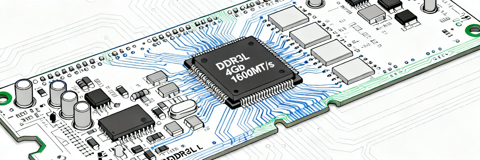
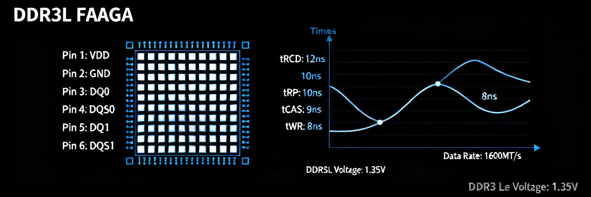
    The MT41K512M8RH-125 delivers a 4Gb device organized as 512M x 8, targeting DDR3-1600 class systems with an I/O clock at 800 MHz and typical access latency near 13.75 ns. It operates at a nominal 1.35V DDR3L voltage, offering a clear voltage and density profile for low-power embedded designs. This datasheet-focused review explains why those headline numbers matter for system architects: power savings relative to standard DDR3, high bit density for constrained board area, and a practical performance envelope for mid-range SoC memory subsystems. Readers will get a concise breakdown of electrical and timing parameters, organization and packaging guidance, PCB integration best practices, a real-world integration scenario, and a compact validation checklist — all framed to support design decisions and verification planning. Key terms used here include the part number and DDR3L class; engineers should treat this as a guided reading of the official datasheet tables and figures for exact test-condition numbers and qualification notes. The article emphasizes which datasheet tables to consult for currents, timing, and mechanical land pattern data and provides actionable recommendations for integration and test. 1 — Product overview & quick spec summary (background) 1.1 — One-line part summary MT41K512M8RH-125 is a 4Gb DDR3L SDRAM organized as 512M x 8 and supplied in an FBGA package class appropriate for high-density BGA mounting. It’s rated for 1.35V operation and an 800 MHz I/O clock (DDR3-1600 class); consult the datasheet mechanical table for exact ball count and footprint class. Action: verify package variant marking against your board footprint early in the BOM review. 1.2 — Typical use cases & compatibility notes This density and voltage class suits mobile modules, embedded controllers, and network-attached SoCs where board area and power matter. DDR3L signals remain electrically compatible with many DDR3 memory controllers with proper voltage/ODS handling; however, confirm controller Vdd/Vddq support and ODT options. Action: map your controller’s supported timing table to the device speed grade before layout. 2 — Key electrical & timing specifications at a glance (data analysis) Parameter / Feature Datasheet Value (MT41K512M8RH-125) Density & Configuration 4Gb (512 Meg x 8) Nominal Supply Voltage (VDD/VDDQ) 1.35V (DDR3L) - Backward compatible with 1.5V I/O Clock / Speed Grade 800 MHz / -125 (DDR3-1600 Class) Internal Banks 8 banks Standard Latency Envelope CL-11-11-11 (tAA = 13.75 ns) Packaging Option 78-ball FBGA (RH variant) 2.1 — Core electrical specs The part’s nominal Vdd/Vddq is 1.35V with defined operating ranges and standby/self-refresh states documented in the datasheet’s electrical characteristics. The datasheet lists currents for active, precharge, and self-refresh modes under specified I/O conditions; use those numbers to size PMIC and decoupling budgets. Action: allocate PDN margin for worst-case active current plus routing loss, and follow the datasheet’s supply-sequencing notes during bring-up. 2.2 — Speed grades & timing (latency) Rated for an 800 MHz I/O clock (DDR3-1600), timing parameters such as tCK, tRCD, tRP and tRAS are provided in timing tables; the datasheet’s typical access time is ~13.75 ns, which maps to system latency expectations at common CAS settings. Impact: tighter CAS and tRCD values reduce latency but tighten timing margins — action: plan for controller calibration and margin analysis using the datasheet timing examples. MT41K512M8RH-125 (512Mx8) VDD/VDDQ (1.35V) VSS/VSSQ (GND) RESET# DQ[7:0] & DQS A[15:0] & BA[2:0] CK / CK# 3 — Memory organization, addressing & packaging details (data analysis) 3.1 — Logical organization & addressing The device organizes memory into multiple banks with row/column addressing consistent with standard DDR3 command sets; data width is x8, so a single device provides eight-bit-wide data lanes. The datasheet specifies burst length, bank count and address mapping tables; check those to size interleaving and rank strategies. Action: align controller address mapping to the device’s bank and row/column scheme to avoid addressing errors. 3.2 — Package & mechanical footprint Packaged in FBGA/BGA, the datasheet includes a mechanical drawing with ball count, pitch, and recommended land pattern; thermal pad and placement notes highlight solder reflow and thermal conduction considerations. Action: match your PCB land pattern and solder mask to the exact datasheet footprint and verify reflow profile against the package thermal limits. 4 — Thermal, reliability & operating conditions (method guide) 4.1 — Operating & storage temperature ranges The datasheet lists commercial and, where available, industrial temperature ranges and corresponding derating guidance. Operating temperature affects refresh rate and retention margin; plan thermal management to keep junction temperature within the specified operating window. Action: simulate worst-case power dissipation and validate board airflow or heatsinking strategies against the datasheet thermal guidance. 4.2 — Reliability metrics & lifecycle considerations Refresh requirements and expected retention behavior are covered in the datasheet; designers should consult the reliability and qualification sections for JEDEC-aligned test flows and any MTBF/qualification notes. Action: include refresh verification and retention stress tests in your qualification plan, and record which datasheet sections govern production test limits. 5 — PCB integration & layout best practices (method guide) 5.1 — Power delivery & decoupling recommendations Follow the datasheet decoupling table for recommended capacitor values and placement: bulk caps on the board edge and high-frequency decouplers close to the package Vdd/Vddq pins. Supply sequencing notes in the datasheet should be implemented by the PMIC. Action: place 0.1µF and higher-frequency caps within millimeters of power pins and verify PDN impedance targets in simulation or lab measurement. 5.2 — Signal routing & termination tips Length-matching for address/command lines and controlled impedance for DQ/DQS are essential; the datasheet suggests ODT settings and termination strategies to reduce reflections. Action: match DQS/DQ groups tightly, use differential routing where required for strobe pairs, and validate signal integrity with IBIS/behavioral models referenced in the datasheet. 6 — Real-world integration example (case display) 6.1 — Example: embedded module memory subsystem Selecting this 4Gb DDR3L part for a mid-performance embedded board balanced density and power: 1.35V operation reduced PDN stress compared to DDR3, while 800 MHz I/O met throughput targets. Key checks included verifying footprint, thermal headroom, and controller timing tables from the datasheet. Action: document these verification checkpoints in the design review. 6.2 — Verification steps performed Bench tests included power-up sequencing verification, write/read margin sweeps, timing calibration runs, and temperature cycling to catch early failures. Each test referenced the datasheet’s electrical and timing tables for pass/fail criteria. Action: capture margin plots and failure logs for regression testing and production sign-off. 7 — Datasheet reading checklist & engineering action plan (action advice) 7.1 — Quick datasheet checklist (engineer’s 8-point list) Confirm part/package variant, voltage ranges and PDN requirements, timing tables required by the memory controller, thermal derating data, footprint match, ODT/termination settings, recommended test patterns, and production qualification notes. Action: map each item to the specific datasheet table or figure during design review and sign off. 7.2 — Common pitfalls & troubleshooting tips Typical fixes include tightening decoupling near power pins when marginal currents appear, reworking address/command length mismatches, and recalibrating ODT/CAS settings for intermittent errors. Action: when encountering instability, reproduce at elevated temperature and log eye/margin metrics against datasheet timing windows. Summary In summary, MT41K512M8RH-125 is a 4Gb (512M x 8) DDR3L device optimized for lower-voltage systems, rated at an 800 MHz I/O class with a typical access time around 13.75 ns. That combination yields meaningful power savings versus legacy DDR3 while delivering high density for area-constrained boards. The datasheet should be your single source for electrical characteristics, timing tables, mechanical footprint, and reliability notes; follow its PDN, decoupling, and routing recommendations and validate with the outlined bench tests to ensure robust integration. Device profile: 4Gb, x8 organization and 1.35V DDR3L operation — confirm package variant and footprint against the datasheet prior to layout. Electrical/timing priorities: consult timing tables for tCK/tRCD/tRP and use the ~13.75 ns access-time figure to set system latency targets and controller calibration. Integration checklist: implement datasheet decoupling and supply sequencing, match trace lengths for DQ/DQS, and run power-up, margin, and thermal stress tests before production. Frequently Asked Questions What is the organization and operating voltage of the MT41K512M8RH-125? The MT41K512M8RH-125 is organized as a 512M x 8 device (4Gb density) operating at a nominal low voltage (DDR3L) of 1.35V, while remaining backward compatible with standard 1.5V environments. How does DDR3L voltage save power compared to standard DDR3? By operating at 1.35V instead of 1.5V, DDR3L reduces thermal overhead and dynamic power dissipation significantly, allowing longer battery life and simplified heat dissipation for embedded modules. What are the key timing parameters for the DDR3-1600 speed grade? The -125 speed grade runs at an 800 MHz clock speed, mapping to DDR3-1600 class performance. Typical access latency (tAA) is 13.75 ns under JEDEC standard CAS settings (CL-11). What routing guidelines apply to DQ and DQS signals? Keep byte lanes grouped together, match routing lengths within standard tolerance bounds, use differential routing for strobe lines (DQS/DQS#), and optimize signal termination (ODT) values to prevent reflections.
  • MT53D512M32D2DS-053 WT:D Спецификации и ключевые характеристики технического описания

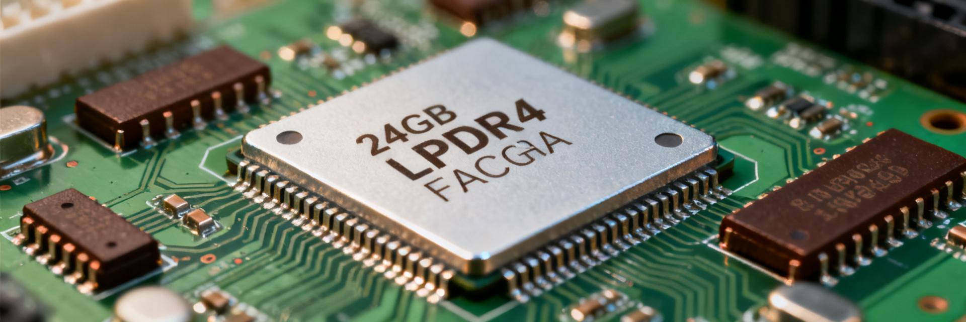
    The MT53D512M32D2DS-053 WT:D is a 16Gb LPDDR4 device organized as 512M x 32 with a rated throughput near 1866 MT/s (≈1.866 GHz clock rate) in a WFBGA package; designers evaluate it for high-bandwidth embedded memory where density, low-power modes, and compact packaging matter. This article translates datasheet tables into actionable design and sourcing guidance to shorten evaluation and reduce integration risk. Expect a concise extraction of headline specs, the electrical and thermal envelope, timing and throughput calculations, package/pinout guidance, validation checklists, and procurement controls — all framed so an engineer can go from datasheet to lab validation efficiently. (1 of 5) — Background & Core Specifications What the part number encodes (organization, density, speed grade) Point: The part string encodes organization, density and speed grade; extracting this lets engineers confirm compatibility with the memory controller. Evidence: MT53D512M32D2DS-053 decodes as 512M×32 organization → 16Gb total, and the suffix indicates the speed grade and package variant. Explanation: confirm the numeric speed-grade (the "-053" suffix) against the official datasheet so timing windows and thermal derates line up with the host controller. Spec Value Density 16 Gb Organization 512M × 32 Nominal I/O voltage ≈1.1 V (LPDDR4 typical) Data-rate ≈1866 MT/s (nominal) Package WFBGA (ball-array) Pin / ball count Refer to datasheet ball-map (verify exact count) Actionable: label this table in the design folder as "MT53D512M32D2DS-053 specs" and copy datasheet figure/table references next to each value for traceability. Electrical & thermal envelope (voltage rails, temp ranges, power modes) Point: LPDDR4 devices list multiple rails (core and I/O), defined operating and storage temperature ranges, and low-power modes. Evidence: expected rails include VDD and VDDQ with typical nominal ~1.1 V; common features: self-refresh, deep power-down and write-leveling support. Explanation: verify the datasheet's operating and storage temperature ranges and note any extended or restricted grades — these affect board thermal design and qualification scope. Actionable: copy the exact VDD/VDDQ ranges and all power-mode currents from the datasheet into the power budget worksheet; include a short note on how tight voltage/timing windows influence SoC PHY compatibility. Use the datasheet as the authoritative source for margining and sequencing steps. (2 of 5) — Data Deep-Dive: Timing, Performance & Reliability Timing parameters & throughput calculations Point: Critical timing parameters (tCK, tRCD, tRP, tRFC, tREFI, DQS timing and CAS latency) determine achievable performance and boot training behavior. Evidence: extract the timing table from the datasheet and cross-check with the memory controller timing window. Explanation: to compute peak theoretical bandwidth use: Bandwidth (GB/s) = (MT/s × bus width in bits) / 8 / 1000 (for GB). Example: 1866 MT/s × 32 bits ÷ 8 = 7.464 GB/s peak per device. MT53D512M32D2DS-053 WT:D 16Gb LPDDR4 (512M x 32) VDD1/VDD2 (1.8V/1.1V) VDDQ (0.6V) VSS/GND DQ[31:0] (Data I/O) DQS[3:0] / CK CA[5:0] (Cmd/Addr) Timing Parameter Notes / Action tCK Copy min/max values from datasheet; validate with PHY CAS / CL Record supported CAS values and training requirements tRFC / tREFI Use for refresh scheduling and controller DRAM maintenance Actionable: annotate the timing table with the host controller limits and flag mismatches before layout; include the datasheet table reference for each number. Reliability, endurance & lifecycle notes Point: Datasheet notes on JEDEC compliance, error-correction support, retention and product status inform long-term use. Evidence: LPDDR4 devices typically state JEDEC conformance and may not include on-die ECC; product status fields indicate active/legacy/obsolete. Explanation: treat "product status" as a procurement risk metric — legacy or obsolete flags require mitigation (alternate sources, redesign windows). Actionable: log any mandatory thermal derating or mandatory cooling requirements in the BOM risk register and flag for sign-off. If MT53D512M32D2DS-053 appears as non-active in the datasheet tables, escalate to procurement immediately. (3 of 5) — Package, Pinout & Integration Guide Package mechanicals & pinout essentials Point: Extract package dimensions, ball-map and mechanical tolerances for footprint verification. Evidence: datasheet mechanical drawings define package size (example dimensions often appear; always verify the exact figure). Explanation: list special pins (power rails, VREF, DQS groups) and call out pitch and critical ball groups for signal integrity checks. Actionable: include a simplified pinout diagram in the hardware folder (referencing the datasheet figure) and attach an SVG/PNG for CAD. Verify land pattern and solder-mask openings against the datasheet's recommended footprint before layout release. PCB layout, signal integrity & power-sequencing best practices Point: Layout and sequencing determine training success and long-term signal integrity. Evidence: best practices include per-rail decoupling, controlled impedance traces for DQ/DQS, and length-matching DQS groups. Explanation: recommend defining plane stackup, placement of bypass capacitors, and a power-sequencing order that meets datasheet Vtt/Vref timing. Actionable: produce a pre-layout checklist (decoupling list, plane stackup, DQS length-matching targets) and a lab validation checklist (scope probe points, training waveform capture, thermal soak test). Double-check required VREF/VTT values in the datasheet before finalizing the power-sequence timeline. (4 of 5) — Performance Use Cases & Benchmarking Typical application scenarios and where this part fits Point: 16Gb LPDDR4 at ~1866 MT/s suits high-throughput embedded applications with tight area and power constraints. Evidence: density and bus width map well to multimedia SoCs, display buffers and networking buffer pools. Explanation: for streaming video or imaging, the device’s peak bandwidth and low-power modes balance throughput and energy; for low-latency tasks, consider controller PHY tuning and bank distribution. Actionable: write short vignettes mapping expected throughput and power trade-offs for each use case and note when multiple die or wider buses are preferable. Benchmark checklist & test-plan highlights Point: A compact benchmark plan verifies datasheet claims and integration sanity. Evidence: tests should measure raw sustained bandwidth, random vs sequential latency, power-per-MB/s, thermal rise under load and training stability. Explanation: capture training logs and PHY calibration behaviors to judge field reliability. Actionable: include a test-plan that logs metrics, fixture description and expected pass/fail criteria; label the document "MT53D512M32D2DS-053 performance" for traceability. (5 of 5) — Design Validation, Compliance & Sourcing Checklist Pre-procurement checklist & life-cycle risk controls Point: Procurement must confirm part-identifier details to avoid mismatches. Evidence: verify full part number and suffix, revision code, temperature grade, package markings and datasheet revision. Explanation: incorrect suffix or revision can change speed grade or temperature limits and invalidate qualification. Actionable: add mandatory line items to the purchase order: datasheet revision reference, product-status confirmation, and incoming inspection criteria (marking, lot code). Perform a board-level validation on first articles prior to design freeze. Migration alternatives and mitigation strategies Point: Plan for replacements and upgrades by identifying which electrical and timing fields must match. Evidence: critical match fields include nominal voltages, timing windows, I/O width and package ball-map. Explanation: some differences can be absorbed in firmware (timing regs), others require hardware changes (VTT, footprint). Actionable: define buffer-stock targets, maintain a cross-reference table for potential replacements, and design firmware abstraction layers to reduce rework risk in the event of end-of-life notices. Summary Core takeaways: the MT53D512M32D2DS-053 WT:D is a 16Gb LPDDR4 device (512M×32) rated near 1866 MT/s in a WFBGA package; designers should prioritize validating the electrical envelope, timing compatibility and sourcing/lifecycle risk before committing to production. Electrical envelope: verify VDD/VDDQ ranges and power-sequence timing from the datasheet into the power budget and BOM risk register. Timing compatibility: extract tCK, CAS, tRFC and DQS timing and compare directly to the SoC PHY; perform the throughput calc and training tests in the lab. Sourcing & lifecycle: confirm full part suffix/revision, datasheet revision, and product status; plan buffer stock and alternate cross-references. Frequently Asked Questions What is the peak bandwidth of MT53D512M32D2DS-053 WT:D? Peak theoretical bandwidth = data-rate × bus width / 8. For 1866 MT/s on a 32-bit bus that equals about 7.464 GB/s. Real sustained bandwidth will be lower; use the benchmark checklist to quantify usable bandwidth under your access pattern. What package and footprint does MT53D512M32D2DS-053 WT:D use? The device is supplied in a WFBGA ball-array package; confirm exact dimensions and ball-map from the datasheet mechanical drawings before PCB layout. Create the footprint per the recommended land-pattern and include solder-mask and paste stencil notes in the CAD files. How to validate timing compatibility with a host controller for MT53D512M32D2DS-053 WT:D? Extract critical timing fields (tCK, tRCD, tRP, tRFC, DQS timing) from the datasheet and compare to the controller's supported windows. Run PHY training, capture DQS eye and latency under representative traffic, and record pass/fail against documented thresholds in the test-plan. What are the primary power supply rails required for this LPDDR4? LPDDR4 typical operation utilizes core rails including VDD1 (typically 1.8V nominal), VDD2 (typically 1.1V nominal), and the I/O rail VDDQ (typically 0.6V nominal). Voltage stability is critical for signal integrity and PHY calibration.
  • Отчет о производительности и подробный анализ LPDDR4 32 Гбайт MT53D1024M32D4DT

    The MT53D1024M32D4DT is a 32Gb LPDDR4 device rated to 2133 MT/s with a x32 I/O (4 bytes/transfer) and ultra-low-voltage core operation (~0.6 V). Translating the headline numbers: 2133 MT/s × 4 bytes = ~8.53 GB/s peak per device, which sets an upper system-bound for a single x32 LPDDR4 package. This report verifies real-world bandwidth, latency, power, and integration trade-offs designers will face when bringing such a device into mobile or embedded platforms. It also prescribes reproducible benchmark methodology and practical PCB, power, and firmware checks so system teams can confirm that datasheet peak figures convert into predictable sustained throughput in their designs. 1 — Background: LPDDR4 32Gb Architecture & Key Specifications What "32Gb" and x32 mean for capacity and bus width Point: "32Gb" denotes gigabits of raw DRAM storage; x32 indicates a thirty-two-bit wide data bus, or four bytes per transfer. Evidence: 32 gigabits equals 4 gigabytes of raw capacity per die; a x32 device delivers four bytes per cycle, so effective peak bandwidth follows transfers×4. Explanation: For designers, a single 32Gb LPDDR4 device typically appears as 4 GB of addressable memory; multi-rank or multi-device assemblies increase capacity or parallelism. Bus width choices (x16 vs x32) affect controller channel mapping, PCB pin count, and achievable peak per-channel throughput. Physical package, voltage rails, and thermal/operating ranges Point: LPDDR4 packages for 32Gb parts are typically small FBGA/QDP with high ball counts and tight footprints; they require multiple low-voltage rails. Evidence: Typical rails include VDD (core), VDDQ (I/O), and a pump or VPP rail where applicable; core voltages approach 0.6 V while I/O commonly sits near 1.05–1.2 V. Explanation: Designers must budget PCB real estate for dense BGA escape routing, place decoupling close to balls, and select power supplies that meet sequencing and transient specs; operating temperature windows differ for consumer versus industrial variants and affect margin requirements. Parameter Specification Details Target Value / Range Density / Capacity Total Addressable Capacity 32Gb (4 Gigabytes) Bus Width Data Interface Configuration x32 (Dual-Channel Architecture) Data Rate Maximum Rated Operational Frequency 2133 MT/s (DDR clock: 1066 MHz) Peak Bandwidth Theoretical Interface Limit ~8.53 GB/s per device Core Voltage (VDD2) Ultra-Low Core Operation Voltage ~0.6 V (Nominal) I/O Voltage (VDDQ) Low-Voltage Swing Interface ~1.1 V / 1.2 V Memory Controller CA [5:0] (Control Bus) DQ [31:0] (Bi-dir Data Bus - 4 Bytes) CK_t / CK_c (Diff. Clock) MT53D1024M32 32Gb LPDDR4 VDD2: 0.6V | VDDQ: 1.1V 2 — Performance Data Deep-Dive: Bandwidth, Latency & Power Calculating theoretical throughput and realistic effective bandwidth Point: Theoretical peak = data rate × bytes per transfer; at 2133 MT/s and x32 that equals ~8.53 GB/s. Evidence: Translating MT/s to bytes/s is straightforward, but effective throughput is reduced by command overhead, refresh, and bus utilization patterns. Explanation: Expect sustained bandwidth in practice to be a fraction of peak—typical sustained ranges for streaming sequential reads are often 60–80% of peak (≈5.1–6.8 GB/s) while random small-block workloads can fall below 30–40% depending on controller efficiency. Use sequential large-block, mixed RW, and random small-block tests to expose those limits. Latency, timing parameters (CAS, tRCD, tRP) and power characterization Point: Timing parameters expressed in cycles map to absolute latency via the device clock period; power has distinct active, standby, and IO components. Evidence: Calculate t(ns) = cycles × (1/MT/s) and measure idle vs active currents with a precision power meter while exercising read/write patterns. Explanation: Higher frequency reduces cycle time and can lower cycle-to-nanosecond conversion but may increase dynamic power. Measure average power under realistic workloads and derive power-per-GB by dividing measured watts by sustained GB/s to compare operating points and trade-offs. 3 — Benchmark Methodology: How to Measure MT53D1024M32D4DT Accurately Testbench, tooling and test vectors Point: Accurate measurement requires a controller or FPGA capable of LPDDR4 training and a precision power/measurement chain. Evidence: Use an FPGA with a validated DDR PHY or a controller evaluation board, a high-speed scope for eye and timing, and a power meter with sub-10 mW resolution plus logic capture for command traces. Explanation: Recommended workloads include sequential large-block streaming, random small-block IOPS, mixed RW at several ratios, and captured real-world traces (multimedia decode, packet buffers) so results map to target applications. Reproducibility, configuration, and reporting standards Point: Reproducible reports require consistent training, sample size, and statistical reporting. Evidence: Run multiple warm-up iterations, perform JEDEC-like training steps, and capture median and 95th-percentile metrics across samples and temperatures. Explanation: Report clock rate, voltage rails, temperature, firmware/timing settings, and error counts; include sample size and run-to-run variance so readers can assess confidence and reproduce the methodology in their labs. 4 — Integration Considerations for System Designers PCB layout, signal integrity and routing best practices Point: Layout dominates whether a 32Gb device hits its throughput and training window. Evidence: Tight trace length matching, controlled impedance, minimized stubs, and optimal placement relative to controller reduce reflections and timing skew. Explanation: Use dedicated DDR routing layers, match fly-by topologies where required, place decoupling capacitors adjacent to power balls, and follow recommended via strategies; poor SI often manifests as failed training or marginal eye diagrams that limit usable data rate. Power delivery, thermal management and firmware/timing tuning Point: Stable low-voltage rails and thermal headroom are prerequisites for rated performance. Evidence: Implement bulk and local decoupling, enforce power-sequence order, and monitor VREF calibration during bring-up. Explanation: During firmware tuning, adjust timing margins, retrain at target temperatures, and use thermal derating to preserve reliability; a bring-up checklist should include VREF calibration, eye checks, and margin testing under worst-case voltage and temperature. 5 — Use Cases, Trade-offs & Procurement/Validation Checklist Target applications and system-level trade-offs Point: A 32Gb LPDDR4 x32 device targets high-bandwidth mobile and embedded systems that need 4 GB per device at relatively low power. Evidence: Suitable applications include image/vision pipelines, network packet buffers, and accelerators that favor single-channel high-throughput memory versus costlier multi-channel solutions. Explanation: Evaluate cost vs capacity, single-die vs multi-die packages, and whether moving to higher-density LPDDR or multiple channels yields better system throughput-per-watt for your workload. Procurement, sample validation and lifecycle considerations Point: Procurement and validation must confirm markings, revisions, and sample adequacy before production. Evidence: Order engineering samples, track part revisions, perform burn-in and stress tests, and validate interoperability with target controllers across temperature. Explanation: A practical checklist should include verifying part marking, sample quantity for statistical confidence, burn-in plans, interoperability matrix, and long-term supply assurances to avoid late-design surprises. Summary In brief, a 32Gb LPDDR4 x32 device operating at 2133 MT/s yields ~8.53 GB/s peak per device, but practical results depend on controller efficiency, layout, timing, and power design. Use the benchmark methodology and integration checklist above to translate datasheet figures into reproducible system metrics and to validate margin across temperature and voltage. Below are concise takeaways and practical next steps for engineering teams. Peak vs sustained: Expect ~8.53 GB/s peak from LPDDR4 x32 at 2133 MT/s, with sustained sequential throughput typically 60–80% of peak; plan system buffers and controller arbitration accordingly. Integration matters: PCB routing, decoupling, and power sequencing strongly influence training success and latency; treat layout and PDN as first-order performance parameters for 32Gb devices. Measurement & validation: Use controlled testbenches, multiple runs, and percentile reporting; validate under worst-case temperature/voltage to ensure MT53D1024M32D4DT-class parts meet system SLAs. Frequently Asked Questions What is the theoretical vs. realistic sustained bandwidth of the MT53D1024M32D4DT? The theoretical peak bandwidth at 2133 MT/s with a x32 bus is approximately 8.53 GB/s. In real-world operation, due to command overhead, refresh cycles, and controller arbitration, designers should expect sustained sequential bandwidth of 60% to 80% of peak (approx. 5.1 to 6.8 GB/s), while random small-block workloads may drop below 30% to 40%. What typical LPDDR4 latency should designers expect and how does it change with frequency? Observed LPDDR4 latency varies with timing settings and operating frequency. Convert cycles to nanoseconds using the transfer period (1/MT/s); increasing frequency shortens cycle time but can increase dynamic power. Designers should measure read/write latency across training points and report median and tail percentiles to capture controller-dependent behavior. How does a 32Gb device impact PCB layout compared with lower-density parts? Higher-density 32Gb packages often increase ball count and require tighter escape routing, making controlled impedance and trace matching more challenging. Place the device close to the controller, minimize stub lengths, and prioritize via strategy and decoupling placement to preserve signal integrity and training margin. What validation steps are essential before qualifying MT53D1024M32D4DT in production systems? Essential validation includes interoperability testing with target controllers, burn-in and stress testing across worst-case temperatures and voltages, VREF calibration and eye diagram margining, and statistical sample runs to verify error-free operation. Document part markings and revision tracking, and confirm long-term availability before final procurement.
  • MT53E768M32D4DT-053 Спецификация: Полные характеристики и схема выводов

    The MT53E768M32D4DT-053 is a 24 Gbit (768M x 32) LPDDR4 mobile memory device rated for high-bandwidth, space-constrained applications. Its top data-rate capability and compact 200-ball FBGA package make it suitable for handheld and embedded designs where power envelope, thermal dissipation, and routing density are critical. This page condenses the official datasheet and a practical pinout guide. This article provides a single-page walkthrough of the datasheet, an interpreted pinout, an integration checklist for PCB layout and SI, and verification tips for engineers. Expect concise tables, an annotated pin grouping summary, layout checklists, and a short validation plan tailored for system integration and risk reduction. 1 — Product snapshot & core specs Key electrical and functional specs Key specs at a glance: density 24 Gbit organized as 768M x 32; LPDDR4 architecture; peak DDR interface clock up to ~1866 MHz (effective data rate dependent on timing grade); supply rails centered on 1.1 V (VDD/VDDQ typical); 200-ball FBGA package; commercial and extended temperature grades noted in the datasheet. Designers should plan for nominal active currents and standby currents with margin when budgeting power. Attribute Value / Note Organization 768M x 32 (24 Gbit) Memory Type LPDDR4 Effective Data Rate Up to ~1866 MHz (device/grade dependent) Voltage VDD / VDDQ ≈ 1.1 V (refer to datasheet) Package 200-ball FBGA Typical Use Mobile, embedded, space-constrained high-bandwidth systems Typical applications & form-factor considerations This device suits smartphones, tablets, compact vision modules, and embedded compute where LPDDR4’s low voltage and high throughput are needed. The FBGA footprint reduces board area but increases thermal and reflow constraints; ensure proper thermal vias and solder-mask clearances. Low-power modes and burst characteristics make it preferable where aggressive power management is required. 2 — Electrical characteristics & timing Power rails, current, and thermal limits VDD and VDDQ nominally target ~1.1 V; absolute ranges and max ratings are defined in the datasheet and must be respected. Typical active and standby currents vary by speed grade—designers should budget for peak write/read current surges plus decoupling headroom. Maintain ambient and junction thermal margins; FBGA thermal path requires plated vias under the die area where specified. Timing parameters and performance (CL, tCK, burst, frequency) Critical timing includes clock period (tCK), CAS-latency equivalents, and burst length behavior. For example, at a 933 MHz clock (1.866 Gbps effective), effective bandwidth per 32-bit device ≈ (1.866 Gbps × 32) / 8 = ~7.464 GB/s theoretical peak. Real achievable throughput is lower due to command overhead, refresh, and controller efficiency—use timing tables to map speed grade to usable bandwidth. MT53E768M32D4DT LPDDR4 24 Gbit SDRAM VDD/VDDQ CA [5:0] CK_t / CK_c CS / CKE DQ [31:0] DQS_t / DQS_c DMI [3:0] 3 — Pinout & package map Annotated pinout diagram: power, address, data, control pins The MT53E768M32D4DT-053 pinout groups power/ground, command/address, data lanes, and reference pins across the FBGA. Power balls (VDD/VDDQ) are distributed to minimize IR drop; GND is abundant. Command/address pins (CS_n, RAS_n, CAS_n equivalents for LPDDR4 command mapping) and CA lanes should be routed with attention to skew. Reset and mode pins must be tied per datasheet sequencing requirements. Pin Group Function / Notes VDD / VDDQ Primary supplies; place local decoupling GND Return plane; short loops CA / CMD Command/address routing; length-matched where required DQ / DQS Data lanes and strobes; strict timing and routing REF / TERM On-die termination reference pins; follow placement guidance PCB footprint and mechanical notes FBGA ball pitch and solder pad dimensions require controlled solder paste volume and mask openings. Recommend thermal via array under the exposed pad area if present; maintain solder-mask expansion per vendor recommendations. Common mistakes: insufficient via stiching, incorrect stencil aperture for center balls, and lack of board warpage control during reflow—use manufacturer footprint notes as the authoritative source. 4 — System integration & layout best practices Power sequencing, decoupling, and rails LPDDR4 parts require defined power-up and power-down sequences; order and timing of VDD/VDDQ and I/O rails affect device reliability. Place multiple decoupling capacitors close to each power ball: bulk capacitance a few millimeters away, high-frequency ceramic 0201/0402 caps within 1–2 mm of pads. Include power-good monitors and test points for VDD, VDDQ, and VTT (if applicable). Signal integrity: routing, termination, and clocking tips Match trace lengths across data strobes and related DQ lines; ensure differential pairs (if applicable) maintain consistent impedance. Place termination resistors near the device where the datasheet recommends and avoid stubs on high-speed nets. Validate with simulation: eye diagrams, channel loss, and crosstalk checks should be part of pre-layout and post-layout verification. 5 — Validation, testing & lifecycle considerations How to validate a board against the datasheet A practical test plan starts with power sequencing verification and passive checks (voltages, continuity). Proceed to controller initialization, then functional memory training at the intended speed grade. Use a logic analyzer, DDR memory controller testbench, and thermal soak to confirm behavior under load. Compare measured currents and timing margins against datasheet tables and log any deviations for corrective layout or firmware changes. Obsolescence, sourcing notes & replacement strategy Confirm lifecycle and obsolescence status via the manufacturer's official part detail page and maintain a cross-reference table in project documentation. If the part becomes unavailable, identify drop-in replacements by matching density, organization, timing grade, voltage, and package. Document rationale for any equivalent part choice and update BOM control files accordingly. Summary The MT53E768M32D4DT-053 summary consolidates the device’s LPDDR4 24 Gb organization, 200-ball FBGA footprint, and power/timing constraints to accelerate design reviews and layout decisions. Use the datasheet’s timing and current tables to size decoupling, set sequencing, and validate thermal strategies early in the design cycle. Follow the provided pin grouping and layout checklist—power placement, short return paths, thermal vias, and matched DQ/DQS routing—to reduce integration risk. Frequently Asked Questions What are the critical power rails and sequencing notes from the MT53E768M32D4DT-053 datasheet? Critical rails include VDD and VDDQ at ~1.1 V; strict sequencing is required to avoid latch-up and to ensure proper device initialization. Designers should verify the datasheet-specified order and delays, place local high-frequency decoupling near power balls, and provide power-good monitoring points. Always test sequencing on a bench before full system bring-up. How should an engineer verify timing and throughput for this LPDDR4 part? Validate timing by running memory controller training at the target speed grade, measure read/write latencies, and capture eye diagrams with an oscilloscope or serial-link tester. Calculate theoretical bandwidth from effective data rate and bus width, then measure sustained throughput under realistic traffic patterns to account for refresh and command overhead. What layout pitfalls commonly cause failures with FBGA LPDDR4 devices? Common failures arise from poor decoupling placement, insufficient thermal vias, mismatched data lane lengths, and inadequate termination placement. Avoid long stubs, keep CA and DQ groups length-matched as specified, and ensure the stencil and solder paste apertures are tuned to prevent tombstoning or voiding on interior balls. What is the peak theoretical bandwidth of the MT53E768M32D4DT-053 LPDDR4? The theoretical peak bandwidth is approximately 7.464 GB/s per 32-bit device. This is derived from an effective clock frequency of 1.866 Gbps running over a 32-bit wide memory interface, computed via the standard formula: (1.866 Gbps * 32) / 8.
  • K4B4G1646E-BMMA Спецификация DDR3L: Полное описание характеристик

    The K4B4G1646E-BMMA device is a 4 Gb DDR3L SDRAM die rated for 1600 MT/s (PC3‑12800 class) with a 1.35 V nominal supply and an extended operating range specified from −40 °C to +95 °C. This guide converts datasheet entries into actionable items for PCB layout, PMIC budgeting, timing configuration and system validation, helping engineers map key rows and tables to real design checkpoints. Read this breakdown to quickly extract package pinout cues, DC/timing limits, thermal and routing constraints, and stepwise bring-up rules. The content emphasizes measurable checks—voltage tolerances, ICC baselines, CAS/tCK mapping and SI validation steps—so teams can reduce bring-up iterations and shorten time to a stable board bring-up. 1 — Quick specs snapshot: K4B4G1646E-BMMA at a glance Key parameters to call out Below is the essential single-line spec breakdown designers need for BOM configuration and initial footprint checking. Parameter Value / Specification Design Relevance Density & Organization 4 Gb (256M x 16) Defines address mapping bounds inside controller registers Speed Class 1600 MT/s (PC3-12800) Sets base timing parameters and routing layout thresholds Supply Voltage (VDD/VDDQ) 1.35V Nominal (DDR3L) Mandates PMIC rail accuracy and decoupling profile Package Type 96-ball FBGA Determines escape routing, trace pitch, and via matrix Operating ranges & grade summary Nominal VDD/VDDQ is 1.35 V with allowed tolerances and device-rated operation down to −40 °C and up to +95 °C. Designers must size PMIC headroom (±5% rail margin typical) and confirm battery or charger operation across the stated thermal extremes to avoid margin loss in low-voltage or industrial systems. 2 — Electrical characteristics & timing: deep dive for system integration K4B4G1646E-BMMA VDD (1.35V) ZQ (240Ω) VSS (GND) DQ [15:0] ADDR/CMD CK / CK# DC electrical specs and currents Datasheet tables list standby and active ICC numbers plus I/O driver levels, VREF and termination currents. Convert ICC peaks into PMIC selection by adding 20–30% margin for worst-case concurrency and translate average current into thermal dissipation to size copper pours and thermal vias. Timing parameters and what they mean (CAS, tRCD, tRP, tRAS, tRFC, tFAW) For 1600 MT/s, tCK is 1.25 ns and typical CAS latencies map to CL9/CL11 in the timing matrix. Calculate effective latency in ns (CL × tCK) to trade off throughput vs latency; prioritize tRFC and tFAW for refresh-heavy workloads and tRCD/tRP for random-access latency tuning. 3 — Performance, signal integrity & DDR3L-specific considerations Bandwidth, command pacing, and throughput sizing Theoretical bandwidth = data rate × bus width (e.g., 1600 MT/s × 16 bits = 3.2 GBytes/s raw per device). Adjust for command, CAS, and refresh overhead—expect sustained throughput to be 70–90% of raw depending on access pattern and controller efficiency. Termination, routing, and signal-integrity checklist Recommended fly‑by topology, controlled impedance traces and on-die termination settings appear in device notes in the DDR3L datasheet. Use 50–60 Ω single-ended and 100–120 Ω differential targets, minimize stubs, validate with SI eye diagrams, and set margin targets for 1600 MT/s operation before production test. 4 — How to apply the DDR3L datasheet to board design and validation Power sequencing, reset, and ZQ calibration steps Verify VDD/VDDQ ramp order, reset assertion windows and ZQ calibration timing as listed in the electrical tables. Implement an automated power-on test that checks rails, measures VREF, performs ZQ calibration and logs timings to validate PMIC sequencing and enable deterministic bring-up. PCB layout, decoupling and thermal management checklist Place decouplers within 2–4 mm of power pins, use multiple bulk and high-frequency caps per rail, add thermal vias beneath the device and verify copper pour balance for reliable thermal dissipation. 5 — Use cases, compatibility pitfalls & implementation checklist Typical system use-cases and compatibility notes Low-voltage DDR3L targets embedded, industrial and mobile-class designs where 1.35 V operation and extended temp are required. Confirm controller supports required address mapping, command timing registers, and separate VTT/VREF domains to avoid address/command bus mismatches and refresh misbehavior. Pre-production validation & troubleshooting flow Bench-level tests include IDD measurements, basic read/write, stress thermal cycling and burn-in per datasheet stress limits. If failures occur, step through voltage tolerance checks, timing misconfiguration scans and termination faults; log failures to isolate between power, SI and controller firmware layers. Summary A focused read of the K4B4G1646E-BMMA DDR3L datasheet yields the essential design inputs—4 Gb density, 1600 MT/s class, 1.35 V nominal and extended temperature limits—necessary to size power, route high-speed nets, and select controller timing parameters. Use the above checklists during schematic capture, PCB layout and bring-up to reduce re-spin risk and shorten time to working silicon. Key Summary: Compact specs: 4 Gb density, 256M x 16 organization, 1600 MT/s rate and 1.35 V class—use one-line spec rows in BOM and schematic checks to prevent footprint mismatches. Power & thermal: Convert ICC numbers to PMIC margin and copper/thermal via budgets; verify rails and ZQ timing during automated bring-up for stability. Layout & SI: Follow fly‑by routing, controlled impedance, minimal stubs and on-die/external termination guidance; validate with eye-diagram targets before production. Common questions and answers How do I map timing tables to controller settings? Read the datasheet timing matrix for the 1600 MT/s bin, derive tCK (1.25 ns) then multiply CL by tCK to get latency in ns. Program CAS, tRCD, tRP, and tRAS consistent with the controller register units and add headroom for temperature-driven timing drift during validation. What are the key power tests to run on bench bring-up? Run rail sequencing checks, measure VDD/VDDQ under no-load and active patterns, verify VREF and termination voltages, perform ZQ calibration and record ICC in standby and active states. Log anomalies to determine PMIC or layout causes before functional tests. Which layout checks catch most DDR3L faults early? Validate controlled impedance, trace length matching for address/command groups, minimized stubs, proper decoupling within millimeters of power pins, and thermal vias under the package. Use pre-layout checklist and an SI review to prevent common signal and power integrity failures. How does 1.35V DDR3L compatibility work with legacy 1.5V host controllers? The K4B4G1646E-BMMA DDR3L device is backward compatible and can operate at 1.5V legacy supply levels. However, you must verify that the host controller and surrounding decoupling network support dual-voltage operation or are correctly locked to the 1.35V domain to achieve power-saving targets.
  • K4B4G1646E-BYMA Техническое описание: Полная схема выводов и временные характеристики

    The K4B4G1646E-BYMA is a high-performance 4Gb DDR3L SDRAM component engineered specifically for low-voltage, high-density system memory architectures. Representing a 256M x16 configuration, this device runs at a nominal 1.35V operational supply, housed within a compact 96-ball FBGA package. Supporting interface speeds up to approximately 933 MHz (DDR3-1866 speed bin), this technical reference synthesizes critical electrical, layout, and timing guidelines to ensure robust design bring-up and physical layer validation. This document distills critical reference metrics from the DDR3L specification into an actionable design guide focusing on timing budgets, ballout grouping, physical layout constraints, and standard validation sequences for FAEs, PCB designers, and signal integrity engineers. 1 — Background & Key Specifications 1.1 — Part Summary & Target Applications Point: The K4B4G1646E-BYMA provides 4Gb density organized in a x16 parallel interface configuration, prioritizing high-bandwidth data transfers in a space-constrained form factor. Evidence: Standard JEDEC specifications register this device within the 96-ball FBGA footprint, utilizing an optimized 1.35V supply while maintaining backward compatibility with 1.5V signaling networks.Explanation: This component is ideally suited for modern embedded architectures, networking platforms, and industrial systems where high-frequency throughput, low standby currents, and compact footprint parameters are mandatory design constraints. 1.2 — Modes of Operation & Variants to Watch Point: The memory array interfaces via flexible JEDEC configurations including DLL enable/disable options, dynamic On-Die Termination (ODT), and write leveling calibration.Evidence: System configuration relies on four internal Mode Registers (MR0–MR3) that program operation modes and address decoding pathways.Explanation: Hardware and firmware development teams must guarantee precise controller configuration of initialization sequences and timing margins to prevent physical bus contention and initialization lockups. 2 — Full Pinout Breakdown 2.1 — Ball/PIN Map & Grouping Point: The 96-ball layout segregates system buses into dedicated geographic zones to minimize signal cross-coupling and facilitate clean routing topologies.Evidence: The interface grouping maps the byte lanes (DQ0–DQ7 and DQ8–DQ15) with their associated lower and upper strobes (LDQS/UDQS), isolating them from the command/address bus. Ball Group Function Key Notes ADDR / CTRL A0–A14, BA0–BA2, RAS#, CAS#, WE# A12/BC# (Burst Chop), A10/AP (Auto-Precharge) CK / CK# Differential Clock Inputs Must be routed as differential pairs with matched impedance DQ / DQS DQ0–DQ15, LDQS, LDQS#, UDQS, UDQS# Matched-length trace grouping required per byte lane VDD / VSS Power and Ground Supply Lines Requires dedicated decoupling loops and low-impedance planes 2.2 — Power Rails, Decoupling & Thermal Pads Point: Correct power delivery network (PDN) decoupling design is critical to avoid voltage drop (IR-drop) during concurrent memory operations.Evidence: Specifications dictate distinct VDD (core voltage) and VDDQ (I/O driver supply) inputs, supplemented by an analog VREF reference line.Explanation: High-frequency ceramic capacitors must reside immediately adjacent to the FBGA power vias. Designers must isolate VREFDQ and VREFCA lines from high-speed digital switching fields to prevent noise-induced signal jitter. CONTROL (ADDR/CMD) CK / CK# / CS# RAS# / CAS# / WE# K4B4G1646E-BYMA (4Gb DDR3L) 256M x 16 Memory Core VDD/VDDQ = 1.35V DATA (DQ/DQS) DQ0 - DQ15 LDQS / UDQS 3 — Timing Parameters Explained 3.1 — Core Timing Glossary Understanding and calculating timing boundaries ensures high-speed signals settle before evaluation cycles: tCK (Clock Cycle Time): Specifies the minimum operational clock period (e.g., ~1.07ns for DDR3-1866). tRCD (RAS to CAS Delay): Internal command interval between active bank command and read/write column access. tRP (Row Precharge Time): Delay constraint to close and precharge an open memory row. tRAS (Active to Precharge Delay): Minimum time to keep a row active before executing precharge routines. CL (CAS Latency): Clock cycles separating the read command receipt from the first output data element. 3.2 — Calculating Timing Margins Point: Absolute clock metrics must account for dynamic operational shifts caused by temperature, voltage fluctuations, and layout skew.Evidence: At 933 MHz (tCK = 1.07 ns), minor layout variations can consume a significant fraction of the unit interval (UI).Explanation: Signal simulation tools must include the physical trace-length delay plus internal silicon propagation delay. Designing with a robust 10–20% margin ensures reliable high-speed data sampling across industrial temperature ranges. 4 — Electrical Characteristics & Power 4.1 — DC/AC Electrical Limits Point: Input signal levels must clear defined threshold metrics to trigger state changes reliably.Evidence: DDR3L specifications define VIL (AC/DC) and VIH (AC/DC) limits around VREF. For 1.35V operational voltages, safety limits contract significantly compared to 1.5V networks.Explanation: Designers must monitor trace termination values and adjust driver strengths (typically via ZQ calibration configurations) to preserve clean signal eyes and limit reflections. 4.2 — Power Consumption & Low-Power Modes Point: Selecting appropriate power states reduces standby thermal strain in modern multi-chip setups.Evidence: Datasheet parameters list distinct active current (IDD0), standby currents, and deep self-refresh profiles.Explanation: Activating the self-refresh mode isolates the external clock line and preserves cell state, shrinking power dissipation to microwatt levels during passive states. 5 — Design Integration & PCB Layout 5.1 — Routing Rules & Signal Integrity Point: Maintaining trace length matches between strobe lines (DQS) and their respective data lines (DQ) is mandatory for data byte synchronization.Evidence: Standard board design paradigms require skew matching down to < 5ps (~25 mil of PCB trace length).Explanation: High-speed clock traces must run as continuous differential microstrip/stripline structures without reference-plane discontinuities. Place series terminating resistors near source drivers if controller dynamic on-die termination (ODT) is bypassed. 5.2 — PCB Case Study: 96-ball FBGA Memory Channel In a standard 8-layer PCB layout stackup, the memory trace design places signal lines on Layers 1 and 3, using Layer 2 as a solid ground reference. All data routes preserve 50Ω single-ended impedance (or 100Ω differential for CK/CK# and DQS/DQS#). Micro-vias routing down from the FBGA pads to internal power planes minimize line inductance, reducing dynamic voltage ripple during dense memory test sequences. 6 — Quick Reference & Validation Checklist 6.1 — Pre-Power Checklist for Bring-up Verify that the VDD and VDDQ power lines are not shorted to ground. Ensure the precision calibration resistor (240Ω ±1%) is correctly terminated on the ZQ pin. Validate that decoupling capacitors are placed as close to the FBGA package pins as routing rules allow. Confirm the VREF resistor divider networks exhibit less than 1% tolerance across operating ranges. 6.2 — Post-Bring-up Tests & Debug Flow Point: Automated software memory tests are required to validate timing margin stability and detect signal-to-noise anomalies.Evidence: Software stress utilities (e.g., Memtest86, custom DMA walk patterns) expose single-bit faults and timing-dependent errors.Explanation: Using high-bandwidth oscilloscopes with BGA-interposers allows engineers to capture raw physical signal eyes. Sweeping read/write delay phases pinpoint margin boundaries across system thermal operating points. Summary & Next Steps Integrating the Samsung K4B4G1646E-BYMA into complex digital designs requires strict adherence to physical layout standards and precise timing calculations. By mapping correct ball configurations, defining exact timing margins, and applying controlled trace layouts, development teams avoid post-production signal integrity issues and ensure long-term physical layer stability. Review the detailed JEDEC standards for edge-case operational states when implementing advanced multi-rank board configurations. Key Summary Confirm power domains and decoupling: VDD, VDDQ, and EPAD routing must meet datasheet recommendations and power sequencing to avoid latch-up and I/O damage. Prioritize strobe and clock routing: Matched DQS-to-DQ grouping and differential CK/CK# pairs are critical for pinout timing and reliable data capture. Validate timing with margins: Convert cycles to nanoseconds at target rates, add 10–20% guard margin, and run DQS phase sweeps and temperature corner stress tests. Common Questions & Answers What are the key pins to watch in the K4B4G1646E-BYMA pinout? Critical pins include CK/CK# clock pairs, DQ groups and matching DQS strobes, address/command control lines, ZQ calibration, and the EPAD power/ground return. Attention to these nets during schematic labeling and board routing prevents timing and power integrity issues during bring-up. How should engineers use the DDR3L datasheet for timing settings? Engineers should extract tCK-based values for CL, tRCD, tRP, tRAS and convert to nanoseconds at the target frequency. Program controller registers with those cycle counts, then apply measured margins via read/write margining and DQS sweep tools to account for board and silicon variances. What are the recommended power sequencing and decoupling guidelines for K4B4G1646E-BYMA? VDD and VDDQ must ramp simultaneously or maintain minimal potential difference. Place decoupling capacitors (typically 0.1µF and 2.2µF ceramic types) directly adjacent to the power pins beneath the 96-ball FBGA to bypass transient high-frequency currents and suppress power distribution network (PDN) noise. What are first-step debug actions for pinout timing failures? Start with eye capture on reads, verify VREF and VDDQ levels, then run DQS phase sweeps and adjust RTT/drive strength. If failures persist, check DQ/DQS length matching, CK routing, and decoupling placement to isolate source of eye closure or timing skew.
  • Спецификации и характеристики MT41K128M16JT-125 DDR3L: Даташит

    Start with headline metrics: the device is a 2 Gbit density arranged as 128M x16, nominal VDD/VDDQ at 1.35 V, and a top speed grade supporting 800 MT/s per pin (effective 1600 MT/s data rate). These numbers matter for low-voltage DRAM in embedded and mobile designs where power and thermal headroom are constrained. This article breaks the MT41K128M16JT-125 datasheet into actionable specs, timing parameters, design guidance, and a procurement checklist. It highlights where to read the AC timing table and DC characteristics, explains MT/s-to-ns conversion, and provides PCB-layout do/don't notes for a reliable DDR3L integration. 1 — Product overview & key electrical specs MT41K128M16JT-125 2Gb (128Mx16) DDR3L CK / CK# CMD / ADDR ODT / CKE DQ [15:0] VDD / VDDQ (1.35V) VSS / VSSQ (GND) Part anatomy & density breakdown Point: The part number encodes a 128M x16 organization equating to 2 Gbit total density and a x16 data bus width. Evidence: Datasheet device organization and package tables list bank count and BGA pin count for the footprint. Explanation: Developers should treat the device as a single x16 SDRAM local to the memory controller or combine multiple devices for wider buses. Parameter Value Density 2 Gbit (128M x16) Data width x16 Typical package FBGA, ball count ≈ 96 (check exact datasheet pinout) Nominal voltages and power rails Point: Nominal VDD/VDDQ is 1.35 V for DDR3L; VPP may be required per specific timing mode. Evidence: DC characteristics table in the datasheet provides standby and active IDD currents and absolute voltage limits. Explanation: Compared with standard DDR3 at 1.5 V, the 1.35 V DDR3L reduces dynamic power roughly proportionally and eases thermal budgets in mobile designs. Rail Typical Notes VDD / VDDQ 1.35 V Operating VPP See DC characteristics If applicable for internal refresh Standby IDD Refer to DC table Budget when in low-power modes 2 — Timing & performance metrics Clock rates, MT/s and effective bandwidth Point: Speed grade lists 800 MT/s per data pin; DDR signaling is double-pumped to give effective 1600 MT/s. Evidence: AC timing table shows tCK and rated MT/s; bandwidth math uses data rate × bus width. Explanation: For x16 device, peak raw bandwidth = 800 MHz × 16 bits = 12.8 Gbit/s; for a 64-bit controller using four devices in parallel, multiply accordingly for system-level throughput. Latencies and common timing parameters (CL, tRCD, tRP, tRAS) Point: CAS latency and tRCD/tRP values appear in the AC timing table and directly impact access latency. Evidence: Typical CL values for the speed grade will be listed (consult the AC timing table). Explanation: Lower CL reduces read latency at the cost of requiring tighter timing margins; designers must cross-check controller timing registers with the datasheet timing values. Timing diagram (simplified): CLK: |¯¯_|¯¯_|¯¯_|¯¯_| ACT : __/‾‾‾\____ CAS : __/‾‾\__ tRCD: tCAS: 3 — Electrical characteristics & signal integrity guidance I/O characteristics and termination Point: I/O uses SSTL signaling with selectable ODT/Rtt options; drive strength and ODT settings affect signal integrity. Evidence: The I/O tables in the DDR3L datasheet enumerate recommended Rtt values and VREF. Explanation: Choose Rtt to match PCB trace impedance, enable ODT where supported to reduce stub reflections, and set VREF per the DC characteristics for reliable reads. Power sequencing, decoupling & thermal considerations Point: Correct power-up/power-down ordering and local decoupling are essential to prevent latch-up or data corruption. Evidence: Power sequencing notes and recommended decoupling in the datasheet indicate cap values and placement. Explanation: Place multiple decoupling caps (e.g., 0.1 µF, 1 µF) close to VDD/VDDQ pins, follow the datasheet power ramp order, and factor thermal derating for high ambient environments. 4 — Integration & PCB layout checklist PCB stackup, routing and via strategy Point: Maintain matched length for data byte lanes and control/address groups; minimize stub lengths and use controlled-impedance traces. Evidence: Layout guidance in the integration notes and signal integrity sections recommend maximum data skew budgets. Explanation: Target per-group length matching within ~50 ps (translate to trace length budget ~10 mm depending on velocity factor), use back-drilled vias where possible, and route data as symmetrical groups to the controller. Reference circuit & pull resistors Point: Reference schematic items include VREF decoupling, recommended pull-up/pull-down ranges, and ESD protection. Evidence: Control pin tables specify acceptable pull resistor ranges and VREF levels. Explanation: Use small series resistors on DQ lines for ringing control, 10–100 kΩ pull resistors on control lines as recommended, and position bulk decoupling near the BGA center to stabilize power rails. 5 — Validation, test patterns & reliability metrics Recommended test vectors and benchmark approach Point: Use deterministic and randomized patterns to validate timing and signal integrity under load. Evidence: Common tests include walking ones/zeros, address march, read-modify-write, and long-run random patterns. Explanation: Run throughput benchmarks at rated speed to verify stability, perform multi-hour burn-in with corner temperature and voltage offsets, and log any bitflips for root-cause analysis. Reliability, temperature and life-cycle considerations Point: Retention, refresh, and temperature class determine long-term behavior and mission profile suitability. Evidence: Operating temperature and retention specifications appear in the datasheet reliability tables. Explanation: Design for appropriate refresh intervals, select parts rated for your operating range (e.g., industrial classes), and monitor soft error rates in field deployments for potential ECC or redundancy needs. 6 — Procurement, compatibility & quick spec checklist Matching part to system requirements Point: Confirm capacity, bus width, speed grade, and voltage compatibility before ordering. Evidence: Cross-reference controller support lists and the device’s electrical/timing tables. Explanation: Verify package constraints for board footprint, ensure controller supports the DDR3L 1.35 V operating point, and confirm the timing grade matches your system clock and latency requirements. Datasheet reading checklist for buyers Confirm speed grade and effective MT/s in the AC timing table. Check operating voltage (VDD/VDDQ), standby IDD, and absolute limits in DC characteristics. Validate CAS latency, tRCD, tRP values in the AC timing table. Verify package type, pinout, and thermal spec for your board footprint. Summary Recap: focus on the critical electrical numbers (2 Gbit, 1.35 V, 800 MT/s per pin), prioritize the AC timing table when setting controller registers, and apply strict PCB routing and decoupling discipline for reliable DDR3L operation. Before sign-off, verify the exact MT41K128M16JT-125 datasheet revision and cross-check timing tables against controller firmware for final specs. Key summary Device density and bus: 128M x16 = 2 Gbit; budget system bandwidth based on effective 1600 MT/s per device and controller bus width. Voltage and power: DDR3L nominal VDD/VDDQ = 1.35 V; audit standby and active IDD in DC characteristics for thermal and battery budgets. Timing priorities: read the AC timing table first—CL, tRCD, tRP directly affect latency; ensure controller timing matches datasheet constraints. FAQ What are the MT41K128M16JT-125 timing parameters I must program? Program CAS latency, tRCD, tRP, and tRAS from the AC timing table for the selected speed grade; these define command-to-data and bank recovery timings. Also set tCK based on the rated MT/s and ensure controller refresh intervals follow the device’s retention and refresh requirements to avoid data loss. How does DDR3L low-voltage 1.35V specs affect PCB decoupling? Lower VDD reduces dynamic power but tightens voltage margin, so place multiple decoupling capacitors close to VDD/VDDQ pins and use low-ESR caps for transient response. Follow datasheet recommendations for bulk and high-frequency decoupling and minimize loop inductance by placing caps on the same PCB side as BGA where possible. Which tests should I run to validate sustained bandwidth and reliability? Run walking ones/zeros, read-modify-write, and long-duration random-access patterns at rated MT/s; combine throughput benchmarks with temperature and voltage corner tests. Use extended burn-in (several hours to days) to reveal marginal timing issues and track error rates to determine if ECC or redundancy is required. Can I run the MT41K128M16JT-125 DDR3L at standard 1.5V DDR3 levels? Yes, the MT41K128M16JT-125 is backward compatible with 1.5V DDR3 signaling systems. However, operating at 1.5V voids the low-power (DDR3L) efficiency advantage and increases thermal dissipation. The memory controller must adjust its I/O drive settings accordingly.