Спецификации и характеристики MT41K128M16JT-125 DDR3L: Даташит
Start with headline metrics: the device is a 2 Gbit density arranged as 128M x16, nominal VDD/VDDQ at 1.35 V, and a top speed grade supporting 800 MT/s per pin (effective 1600 MT/s data rate). These numbers matter for low-voltage DRAM in embedded and mobile designs where power and thermal headroom are constrained.
This article breaks the MT41K128M16JT-125 datasheet into actionable specs, timing parameters, design guidance, and a procurement checklist. It highlights where to read the AC timing table and DC characteristics, explains MT/s-to-ns conversion, and provides PCB-layout do/don't notes for a reliable DDR3L integration.
1 — Product overview & key electrical specs
Part anatomy & density breakdown
Point: The part number encodes a 128M x16 organization equating to 2 Gbit total density and a x16 data bus width. Evidence: Datasheet device organization and package tables list bank count and BGA pin count for the footprint. Explanation: Developers should treat the device as a single x16 SDRAM local to the memory controller or combine multiple devices for wider buses.
| Parameter | Value |
|---|---|
| Density | 2 Gbit (128M x16) |
| Data width | x16 |
| Typical package | FBGA, ball count ≈ 96 (check exact datasheet pinout) |
Nominal voltages and power rails
Point: Nominal VDD/VDDQ is 1.35 V for DDR3L; VPP may be required per specific timing mode. Evidence: DC characteristics table in the datasheet provides standby and active IDD currents and absolute voltage limits. Explanation: Compared with standard DDR3 at 1.5 V, the 1.35 V DDR3L reduces dynamic power roughly proportionally and eases thermal budgets in mobile designs.
| Rail | Typical | Notes |
|---|---|---|
| VDD / VDDQ | 1.35 V | Operating |
| VPP | See DC characteristics | If applicable for internal refresh |
| Standby IDD | Refer to DC table | Budget when in low-power modes |
2 — Timing & performance metrics
Clock rates, MT/s and effective bandwidth
Point: Speed grade lists 800 MT/s per data pin; DDR signaling is double-pumped to give effective 1600 MT/s. Evidence: AC timing table shows tCK and rated MT/s; bandwidth math uses data rate × bus width. Explanation: For x16 device, peak raw bandwidth = 800 MHz × 16 bits = 12.8 Gbit/s; for a 64-bit controller using four devices in parallel, multiply accordingly for system-level throughput.
Latencies and common timing parameters (CL, tRCD, tRP, tRAS)
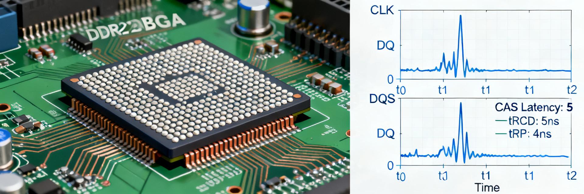
Point: CAS latency and tRCD/tRP values appear in the AC timing table and directly impact access latency. Evidence: Typical CL values for the speed grade will be listed (consult the AC timing table). Explanation: Lower CL reduces read latency at the cost of requiring tighter timing margins; designers must cross-check controller timing registers with the datasheet timing values.
Timing diagram (simplified):
  CLK: |¯¯_|¯¯_|¯¯_|¯¯_|
  ACT :   __/‾‾‾\____
  CAS :      __/‾‾\__
  tRCD: <---- tRCD ---->
  tCAS: <-------- CL -------->
3 — Electrical characteristics & signal integrity guidance
I/O characteristics and termination
Point: I/O uses SSTL signaling with selectable ODT/Rtt options; drive strength and ODT settings affect signal integrity. Evidence: The I/O tables in the DDR3L datasheet enumerate recommended Rtt values and VREF. Explanation: Choose Rtt to match PCB trace impedance, enable ODT where supported to reduce stub reflections, and set VREF per the DC characteristics for reliable reads.
Power sequencing, decoupling & thermal considerations
Point: Correct power-up/power-down ordering and local decoupling are essential to prevent latch-up or data corruption. Evidence: Power sequencing notes and recommended decoupling in the datasheet indicate cap values and placement. Explanation: Place multiple decoupling caps (e.g., 0.1 µF, 1 µF) close to VDD/VDDQ pins, follow the datasheet power ramp order, and factor thermal derating for high ambient environments.
4 — Integration & PCB layout checklist
PCB stackup, routing and via strategy
Point: Maintain matched length for data byte lanes and control/address groups; minimize stub lengths and use controlled-impedance traces. Evidence: Layout guidance in the integration notes and signal integrity sections recommend maximum data skew budgets. Explanation: Target per-group length matching within ~50 ps (translate to trace length budget ~10 mm depending on velocity factor), use back-drilled vias where possible, and route data as symmetrical groups to the controller.
Reference circuit & pull resistors
Point: Reference schematic items include VREF decoupling, recommended pull-up/pull-down ranges, and ESD protection. Evidence: Control pin tables specify acceptable pull resistor ranges and VREF levels. Explanation: Use small series resistors on DQ lines for ringing control, 10–100 kΩ pull resistors on control lines as recommended, and position bulk decoupling near the BGA center to stabilize power rails.
5 — Validation, test patterns & reliability metrics
Recommended test vectors and benchmark approach
Point: Use deterministic and randomized patterns to validate timing and signal integrity under load. Evidence: Common tests include walking ones/zeros, address march, read-modify-write, and long-run random patterns. Explanation: Run throughput benchmarks at rated speed to verify stability, perform multi-hour burn-in with corner temperature and voltage offsets, and log any bitflips for root-cause analysis.
Reliability, temperature and life-cycle considerations
Point: Retention, refresh, and temperature class determine long-term behavior and mission profile suitability. Evidence: Operating temperature and retention specifications appear in the datasheet reliability tables. Explanation: Design for appropriate refresh intervals, select parts rated for your operating range (e.g., industrial classes), and monitor soft error rates in field deployments for potential ECC or redundancy needs.
6 — Procurement, compatibility & quick spec checklist
Matching part to system requirements
Point: Confirm capacity, bus width, speed grade, and voltage compatibility before ordering. Evidence: Cross-reference controller support lists and the device’s electrical/timing tables. Explanation: Verify package constraints for board footprint, ensure controller supports the DDR3L 1.35 V operating point, and confirm the timing grade matches your system clock and latency requirements.
Datasheet reading checklist for buyers
- Confirm speed grade and effective MT/s in the AC timing table.
- Check operating voltage (VDD/VDDQ), standby IDD, and absolute limits in DC characteristics.
- Validate CAS latency, tRCD, tRP values in the AC timing table.
- Verify package type, pinout, and thermal spec for your board footprint.
Summary
Recap: focus on the critical electrical numbers (2 Gbit, 1.35 V, 800 MT/s per pin), prioritize the AC timing table when setting controller registers, and apply strict PCB routing and decoupling discipline for reliable DDR3L operation. Before sign-off, verify the exact MT41K128M16JT-125 datasheet revision and cross-check timing tables against controller firmware for final specs.
Key summary
- Device density and bus: 128M x16 = 2 Gbit; budget system bandwidth based on effective 1600 MT/s per device and controller bus width.
- Voltage and power: DDR3L nominal VDD/VDDQ = 1.35 V; audit standby and active IDD in DC characteristics for thermal and battery budgets.
- Timing priorities: read the AC timing table first—CL, tRCD, tRP directly affect latency; ensure controller timing matches datasheet constraints.
FAQ
What are the MT41K128M16JT-125 timing parameters I must program?
Program CAS latency, tRCD, tRP, and tRAS from the AC timing table for the selected speed grade; these define command-to-data and bank recovery timings. Also set tCK based on the rated MT/s and ensure controller refresh intervals follow the device’s retention and refresh requirements to avoid data loss.
How does DDR3L low-voltage 1.35V specs affect PCB decoupling?
Lower VDD reduces dynamic power but tightens voltage margin, so place multiple decoupling capacitors close to VDD/VDDQ pins and use low-ESR caps for transient response. Follow datasheet recommendations for bulk and high-frequency decoupling and minimize loop inductance by placing caps on the same PCB side as BGA where possible.
Which tests should I run to validate sustained bandwidth and reliability?
Run walking ones/zeros, read-modify-write, and long-duration random-access patterns at rated MT/s; combine throughput benchmarks with temperature and voltage corner tests. Use extended burn-in (several hours to days) to reveal marginal timing issues and track error rates to determine if ECC or redundancy is required.
Can I run the MT41K128M16JT-125 DDR3L at standard 1.5V DDR3 levels?
Yes, the MT41K128M16JT-125 is backward compatible with 1.5V DDR3 signaling systems. However, operating at 1.5V voids the low-power (DDR3L) efficiency advantage and increases thermal dissipation. The memory controller must adjust its I/O drive settings accordingly.