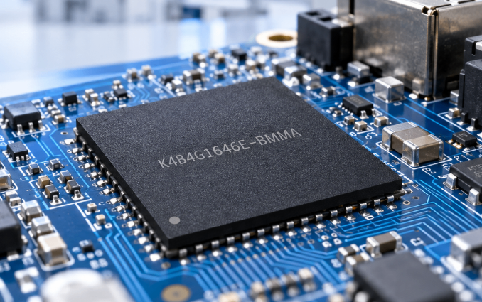
MT40A512M16LY-062E DDR4 Datasheet: Deep Specs & Metrics
Introduction: This high-density SDRAM building block is designed for server, industrial, and embedded memory subsystems, featuring peak transfer capabilities tied to DDR4 speed standards and a highly efficient per-device x16 organization. When integrating this IC, engineers must tightly map datasheet parameters to board-level constraints to prevent layout re-spins and ensure adequate power, timing, and thermal margins.
This technical analysis extracts actionable design rules from the MT40A512M16LY-062E configuration datasheet, enabling hardware engineers to quickly translate electrical values into practical power budgets, timing parameters, and layout guidelines.
1 — Overview: What MT40A512M16LY-062E Is and Where It Fits
— Memory Organization & Part Identity
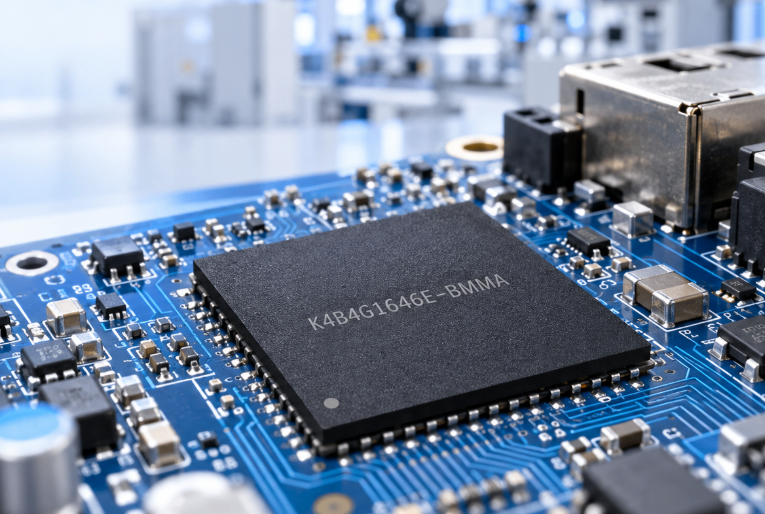
The MT40A512M16LY-062E is an 8Gb DDR4 SDRAM device organized as a 512 Meg x 16 configuration. The part number maps directly to its architecture: "MT40A" indicates Micron's DDR4 family, "512M16" defines the depth and width configuration, "LY" signifies its physical package attributes (96-ball FBGA package), and "-062E" establishes the clock speed grade at DDR4-3200 with CL=22 latency. Designers must verify these identifiers in the procurement chain to ensure drop-in physical and functional compatibility.
— Typical Target Applications and Performance Class
Due to its high bandwidth and 16-bit wide bus organization, this memory device is optimized for performance-critical embedded systems, edge-computing nodes, and server interface modules. When evaluating "MT40A512M16LY-062E use cases," the device is often selected over low-power alternatives (LPDDR) for platforms requiring sustained memory bandwidth, standard 1.2V compatibility, and wide thermal margins under high-duty cycle compute loads.
2 — Electrical Specifications & Pinout Essentials
— Supply Rails, I/O Voltages, and Power Consumption Metrics
The primary power rails driving the device are VDD (core supply at 1.2V), VDDQ (I/O supply at 1.2V), and VPP (activation supply at 2.5V). To size power regulators accurately, system developers should refer to the maximum operating currents (IDD metrics) outlined in the DDR4 datasheet.
| Operating Parameter | Symbol / Condition | Typical Value | Unit |
|---|---|---|---|
| Core Operating Voltage | VDD | 1.20 (± 0.060) | V |
| I/O Operating Voltage | VDDQ | 1.20 (± 0.060) | V |
| Wordline Boost Voltage | VPP | 2.50 (min 2.375) | V |
| Operating Current (Burst Read) | IDD4R (at DDR4-3200) | 145 | mA |
| Operating Current (Burst Write) | IDD4W (at DDR4-3200) | 138 | mA |
| Active Standby Current | IDD3N | 43 | mA |
— Pinout, Package, and Signal Naming
The physical 96-ball FBGA footprint dictates strict PCB routing escapes. Crucial control lines including On-Die Termination (ODT), Clock Enable (CKE), and Active-Low Reset (RESET#) require careful passive termination and precise sequence control to prevent state corruption during startup and initialization phases.
3 — Timing, Latency, and Performance Analysis
— Supported Frequencies, Transfer Rates, and Timing Parameters
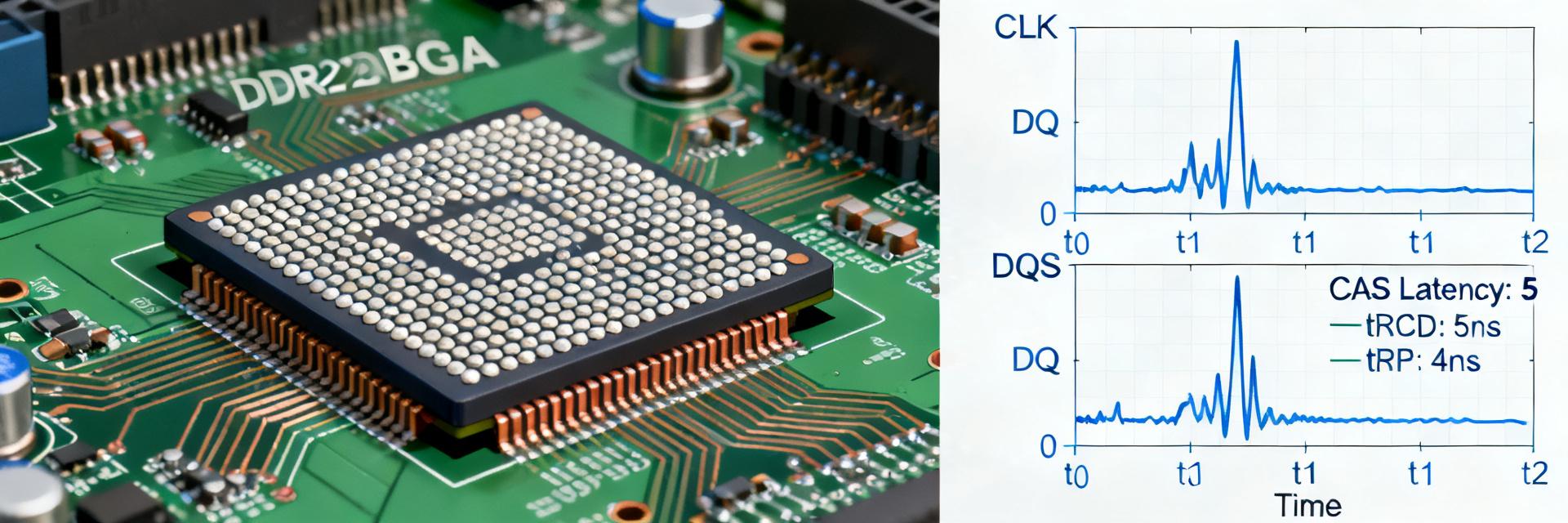
The speed grade "-062E" indicates compliance with DDR4-3200 JEDEC standards (data rate of 3200 MT/s). Translating raw cycle metrics into physical time values ensures the memory controller is properly configured:
- tCK (Minimum Clock Period): 0.625 ns
- tAA (CAS Latency - CL): 22 cycles (equivalent to 13.75 ns)
- tRCD (RAS to CAS Delay): 22 cycles (13.75 ns)
- tRP (Row Precharge Time): 22 cycles (13.75 ns)
— Bandwidth, Throughput, and Real-World Implications
The maximum theoretical bandwidth for a single x16 device is calculated as:
Bandwidth = 3200 MT/s × 16 bits / 8 bits per byte = 6.4 GB/s.
In physical system scenarios, actual data throughput is reduced by command overhead, periodic refresh cycles (tREFI), and page conflicts. Designers should apply a 20% efficiency derating factor (targeting 75% to 80% real-world efficiency) when modeling data bus loading.
4 — Signal Integrity, Timing Margins & Layout Recommendations
— SI Considerations: Termination, DQ/DQS Routing, and Impedance Control
Operating high-speed signals at 1600 MHz requires careful PCB layout and routing:
Maintain 50Ω single-ended impedance for signal lines and 100Ω differential impedance for critical clock (CK) and strobe (DQS) pairs. Keep skew mismatch between DQ and DQS trace lengths under 10 mils within the same byte lane to preserve setup and hold margins.
— Thermal and Reliability Parameters
The operating temperature (TC) ranges from 0°C to 95°C. When operating above 85°C, the refresh rate must double (tREFI drops from 7.8 µs to 3.9 µs) to prevent data corruption. For high-temperature environments, implementing thermal vias, thick copper planes, and forced airflow is essential to maintain junction temperatures within safe limits.
5 — Integration Checklist: Power Sequencing, Reset, and PCB Considerations
— Power-Up/Power-Down Sequencing and Reset Timing
To avoid latch-up and prevent input buffer damage, the power rails must ramp up in a specific order: VPP must stabilize before or concurrently with VDD, and VDDQ must follow VDD. The RESET# signal must remain low for a minimum of 200 µs after power rails stabilize, and CKE must be pulled low before releasing RESET#.
— BOM & Footprint Best Practices
Place 0.1 µF high-frequency decoupling capacitors directly underneath the memory footprint, close to individual VDD and VDDQ pins. Use a 96-ball land pattern designed to compensate for solder mask expansion and joint reliability, ensuring the component's footprint matches the physical "LY" package specification exactly.
6 — Validation, Testing, and Selecting the Right Variant
— Test Vectors, Compliance, and Qualification Steps
System qualification requires validation of high-speed signals and timing margins:
Use real-time oscilloscopes with memory compliance software to capture DQ eye-diagrams, and verify that setup and hold times meet JEDEC specifications. Execute extensive Bit Error Rate (BER) tests using multi-pattern diagnostic software (such as Memtest86+ or custom DDR stress scripts) under extreme operating temperatures.
— How to Read Datasheet Revisions and Choose Between Part Variants
Always review the revision history of the datasheet to track changes to electrical parameters, active current tables, and mechanical package updates. When migrating between speed grades (e.g., from -075 to -062E), verify that the memory controller's physical layer (PHY) can support the higher frequency while maintaining the correct timing margins.
Summary
- High-Density x16 Architecture: The MT40A512M16LY-062E provides 8Gb of high-speed memory capacity in a compact 96-ball FBGA package, optimized for high-bandwidth embedded systems.
- Standardized Timing & Power: Operates at 1.2V (VDD/VDDQ) with standard DDR4-3200 CL-22-22-22 timings, delivering up to 6.4 GB/s of raw bandwidth per device.
- Strict Signal Integrity: Requires 50Ω single-ended / 100Ω differential impedance control, matched trace lengths, and robust decoupling layouts to ensure stable, noise-free performance.
FAQ
What are the critical MT40A512M16LY-062E timing parameters to extract from the DDR4 datasheet?
The critical timing parameters to extract are tCK (0.625ns for DDR4-3200), CL (22 cycles), tRCD (13.75ns), and tRP (13.75ns). These parameters are crucial for programming the memory controller and calculating the exact latency overhead of random and sequential access cycles.
How should engineers build a power budget using MT40A512M16LY-062E specs?
Engineers should extract state-specific IDD values from the datasheet (e.g., IDD0 for operating current, IDD4R/W for burst read/write, and IDD5B for burst refresh), multiply these currents by the system voltage rails (VDD=1.2V, VPP=2.5V), scale by the duty cycle of active devices, and add a safety margin of 20-30% for regulator thermal losses.
What PCB layout rules preserve signal integrity for this high-speed memory interface?
Maintain 50-ohm single-ended (or 100-ohm differential for DQS/CK) impedance control, strictly match trace lengths within byte lanes (DQ to DQS) to under 10 mils, avoid signal stubs, implement continuous ground return planes directly beneath high-speed signals, and place decoupling capacitors as close as possible to the device power pins.
What validation steps ensure the chosen MT40A512M16LY-062E variant meets system needs?
A robust validation plan includes executing high-stress read/write test patterns, conducting voltage and timing margin sweeps (shmoo plots), performing signal integrity scope captures on DQ/DQS lines, and conducting thermal cycling tests to monitor the Bit Error Rate (BER) and ensure zero-fault operation across the target environmental range.