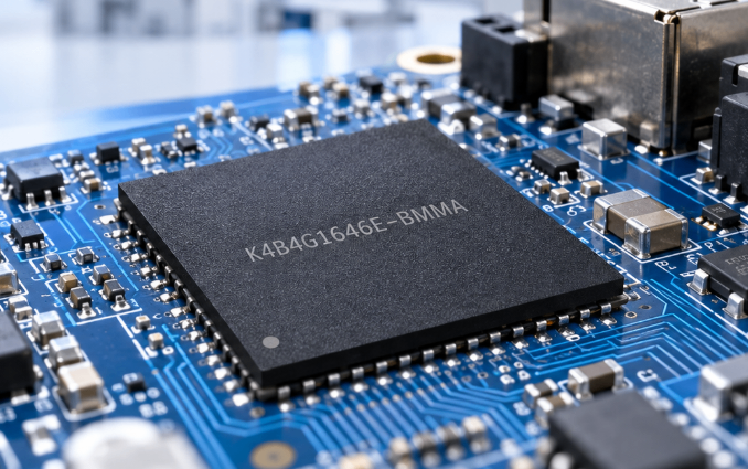
MT40A1G16KD-062E DDR4: Deep Datasheet Analysis & Key Specs
The MT40A1G16KD-062E is a 16‑Gbit DDR4 device specified for 3200 MT/s (1600 MHz effective), VDD/VDDQ ≈ 1.2 V, x16 device width and CAS latency points around CL22, yielding ~6.4 GB/s raw per device. This opening statement frames the actionable breakdown below for electrical, timing and board‑level implications derived from the official datasheet and measured practice.
| Specification Parameter | Datasheet Nominal Values | Design Consideration & Margin |
|---|---|---|
| Density & Organization | 16 Gbit (1G x 16) | Directly impacts bank parallelism & controller width |
| VDD / VDDQ Rails | 1.2V (Nominal) | Tight voltage stability required; trace width calibration |
| VPP Pump Supply | 2.5V (Nominal) | Must satisfy sequence start thresholds before initialization |
| Clock Speed & Transfer Rate | 1600 MHz / 3200 MT/s | CL22 latency metrics match typical 0.625ns tCK parameters |
| Operating Temp Range | –40 °C to +95 °C | Thermal derating protocols apply over 85°C thresholds |
1 — Part overview & key electrical / mechanical specs (background)
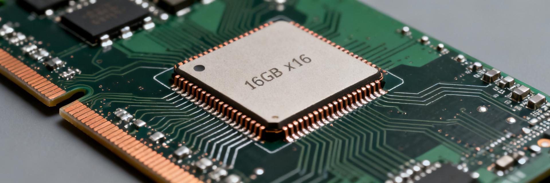
Point: A concise part overview helps capacity planning and channel mapping. Evidence: The device is a 16 Gbit x16 DDR4 SDRAM organized into internal banks and bank groups. Explanation: Engineers should map logical arrays to system channels to calculate ranks per channel and total DIMM capacity when populating x16 devices in multi‑rank assemblies.
1.1 Memory organization & density
Point: Organization affects latency, refresh and rank behavior. Evidence: The die presents 16 Gbit total in x16 format with multiple internal banks and bank groups typical of DDR4 architectures. Explanation: Designers must account for bank parallelism when designing interleaving and consider x16 width when selecting controller data path width for bandwidth aggregation.
1.2 Electrical rails, package & environmental limits
Point: Power rails and thermal margins drive sequencing and BOM. Evidence: Nominal VDD/VDDQ ≈ 1.2 V, VPP required for internal charge pumps, pseudo‑open‑drain I/O signaling and compact FBGA packaging with commercial operating range around –40 °C to +95 °C per datasheet. Explanation: Budget VDD rail noise, plan VPP sequencing, place decoupling adjacent to the package and verify reflow profile for the specified ball count and pitch.
2 — Performance parameters & timing analysis (data analysis)
Point: Compute usable throughput and understand overheads. Evidence: Peak single‑device raw throughput = 3200 MT/s × 16 bits ÷ 8 = 6.4 GB/s. Explanation: Effective throughput will be lower due to command overhead, refresh windows and multi‑rank arbitration; system designers must convert MT/s into sustained bandwidth using realistic efficiency factors (typically 60–85% depending on workload).
2.1 Speed, bandwidth & how to compute usable throughput
Point: A repeatable formula simplifies planning. Evidence: Throughput formula (transfers/s × bus width / 8) yields raw numbers; example single device gives ~6.4 GB/s. Explanation: For multi‑rank/channel scenarios, multiply by ranks per channel and account for controller inefficiencies and protocol overhead to produce realistic system bandwidth projections for benchmarks and thermal load estimation.
2.2 Timing parameters and latency implications
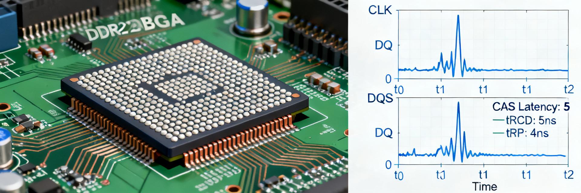
Point: Timing fields govern latency and margin. Evidence: Key timing values include CL, tRCD, tRP, tRAS and tCK; latency in ns = CL × tCK. Explanation: Translate CL22 at a tCK of 0.625 ns (for 1600 MHz) into approximate access latency and monitor tRCD/tRP during bring‑up; these are primary levers for firmware timing tuning and margin analysis against the datasheet timing tables.
3 — Signal integrity, calibration & voltage reference considerations (method/guide)
Point: VREFDQ calibration and signaling topology determine data eye quality. Evidence: The device provides on‑die adjustable VREFDQ for DQ sampling and uses pseudo‑open‑drain I/O requiring proper termination. Explanation: Set VREF near 0.5×VDDQ, run training sequences to center the eye and log eye height/width during initialization; mismatched VREF is a frequent root cause of intermittent CRC or data errors.
3.1 VREFDQ, on‑die calibration & I/O signaling notes
Point: Calibration order and margins matter on first boot. Evidence: On‑die VREF adjustments and DQ/DQS timing training are described in the part documentation. Explanation: Recommended practice is to establish stable VDD/VDDQ, perform VREF training early, then run DQS gate and read leveling; capture VREF and DQ eye metrics to validate controller training sequences and reportability.
3.2 Power sequencing, decoupling & thermal handling
Point: Sequencing and decoupling minimize noise and maintain timing margin. Evidence: Datasheet calls out VDD/VDDQ/VPP sequencing constraints and decoupling guidelines; thermal derating applies at high ambient. Explanation: Use tiered decoupling (bulk, mid, local) and ensure VPP is present at the point required by the recommended sequence; instrument VDD ripple and hot‑spot temperature during stress tests.
4 — Package, board integration & PCB layout checklist (case / integration)
Point: Footprint and critical nets drive layout constraints. Evidence: The package uses high‑density ball grid arrays with critical nets DQS, DQ, CK, CA, VREF and multiple power balls. Explanation: Prioritize escape routing, via‑in‑pad mitigation, and keep DQS close to DQ lanes; define clear land patterns and follow reflow recommendations consistent with the package family identifier in the part documentation.
4.1 Package footprint, pin‑out considerations & land‑pattern notes
Point: Early layout reviews prevent costly respins. Evidence: Critical nets and soldering profile notes appear in the part’s mechanical appendices. Explanation: Verify ball mapping against controller pin assignments, plan thermal vias under ground planes carefully, and confirm solder paste stencil and reflow profile to avoid solder voiding and ensure reliable joints on high‑density FBGA packages.
4.2 Routing, length matching & termination checklist
Point: Routing topology controls timing skew and reflections. Evidence: Flyby topology for address/command and fly‑by or DDR4 recommended DQ/DQS alignment guidance are in reference materials. Explanation: Match DQS to DQ within tight tolerances (tens of picoseconds), use controlled impedance traces, place series termination as needed, and prefer symmetric plane stackups to minimize mode conversion and crosstalk.
5 — Validation procedures, test modes & troubleshooting checklist (action recommendations)
Point: Structured validation isolates electrical vs firmware issues. Evidence: Test modes such as self‑refresh, power‑down and IDD measurement points are specified in the datasheet. Explanation: Execute a step‑by‑step bring‑up: verify power sequencing, run training, measure IDD in each mode and exercise refresh behavior; log failures with scope captures of DQS/DQ and VREF levels to triage root causes quickly.
5.1 Test modes, refresh behavior & power/sequence validation
Point: Use datasheet test vectors to confirm conformance. Evidence: Self‑refresh, low‑power and standard operating modes have defined timing and current signatures. Explanation: Validate refresh intervals, confirm IDD values within expected windows, and run deterministic read/write patterns that exercise row hammer and long‑hold scenarios to ensure stable retention and correct power‑down transitions.
5.2 Common failure modes & targeted debug steps
Point: Targeted measurements speed debug. Evidence: Typical failures manifest as training failures, CRC/data corruption or timing margin shortfalls referenced by the datasheet examples. Explanation: Capture DQS/DQ waveforms with a high‑bandwidth scope, probe VREF and VDD ripple, increment timing margins in firmware, and improve decoupling or trace impedance to recover reliability as first‑order mitigations.
Summary
MT40A1G16KD-062E is a 16Gb DDR4 x16 device rated for 3200 MT/s with on‑die VREFDQ and ~1.2 V rails; primary integration tasks are timing verification, VREF calibration and careful PCB routing. Use the timing, power and layout guidance above as a checklist when moving from the published datasheet to board bring‑up and validation phases.
- Prioritize timing validation: compute latency (ns = CL × tCK) and verify tRCD/tRP margins under stress to ensure reliable read/write operations and predictable performance.
- Calibrate VREFDQ early: set VREF near mid‑rail, run training sequences and log eye metrics; VREF misadjustment is a common cause of transient errors.
- Follow PCB layout rules: control impedance, match DQS/DQ lengths tightly, place decoupling tiers close to power balls and respect flyby topology for CA lines.
Common Questions & Answers
What are the key MT40A1G16KD-062E electrical rails and tolerances?
The primary rails are VDD and VDDQ at approximately 1.2 V with a separate VPP for internal functions; tolerances and recommended sequencing are specified in the official part documentation. Designers must budget for ripple, place local decoupling and verify rail timings during bring‑up to prevent initialization faults and timing drift.
How does CL translate to latency for this DDR4 device?
Latency in nanoseconds equals CL multiplied by tCK; for example CL22 at a tCK of 0.625 ns yields roughly 13.75 ns raw CAS latency. Engineers should add tRCD and command overhead to estimate end‑to‑end read latency and validate these numbers against observed turnaround times during system benchmarks.
What are the fastest debug steps for training failures with this DDR4 device?
Capture DQS/DQ with a high‑bandwidth scope, confirm VREF and VDD stability, increase timing margins in firmware and improve decoupling near the device. If reflections appear, review termination and trace impedance; repeated training failures often trace to VREF miscalibration or power sequencing anomalies that are corrected by adjusting order and improving local decoupling.
What routing topology is recommended for MT40A1G16KD-062E high-speed signals?
Flyby topology is recommended for address/command lines, paired with tight length matching (within tens of picoseconds) between DQS and DQ lanes. Designers should maintain controlled impedance traces, utilize proper series termination, and implement symmetric PCB plane stackups to minimize crosstalk and mode conversion.