DDR3L 4Gb Parts Breakdown: Specs, Pinouts & Benchmarks
Point: DDR3L 4Gb remains a practical choice for legacy laptops, embedded modules and cost-sensitive designs due to its low-voltage 1.35V footprint and wide availability. Evidence: System-level power budgets and module inventories frequently show DDR3L as the common low-voltage option for single-rank SODIMMs and soldered-down arrays. Explanation: This article delivers clear DDR3L 4Gb specs, pinout guidance and practical benchmark recommendations to help engineers and technical buyers select and validate parts efficiently.
Point: Readers should expect actionable device organization notes, electrical basics, benchmark methodology and bench-to-production checklists. Evidence: Each section synthesizes typical datasheet parameters, package pin maps and measurement points used in qualification labs. Explanation: Follow the sections in order to translate device density into module capacity, assess performance by speed grade, and validate parts from prototype to production.
DDR3L 4Gb — architecture & core specs (Background)
Density, organization & addressing (x4 / x8 / x16)
Point: "4Gb" denotes four gigabits per device and organization determines the data bus width and how many devices produce a given module capacity. Evidence: Typical organizations for 4Gb parts are 256M x16 or 512M x8 (logical equivalence), with bank and row/column addressing shown in manufacturer datasheets. Explanation: Translate device count to module bytes by summing device widths per rank (e.g., eight x4 devices yield a x32 data path); use organization to plan rank/channel topology for the memory controller.
| Configuration | Addressing Structure | Bank Count | Page Size |
|---|---|---|---|
| 512M x 8 | 16 Rows x 10 Columns | 8 Banks | 1 KB |
| 256M x 16 | 15 Rows x 10 Columns | 8 Banks | 2 KB |
Voltage, timing & electrical basics (1.35V, CL, data rates)
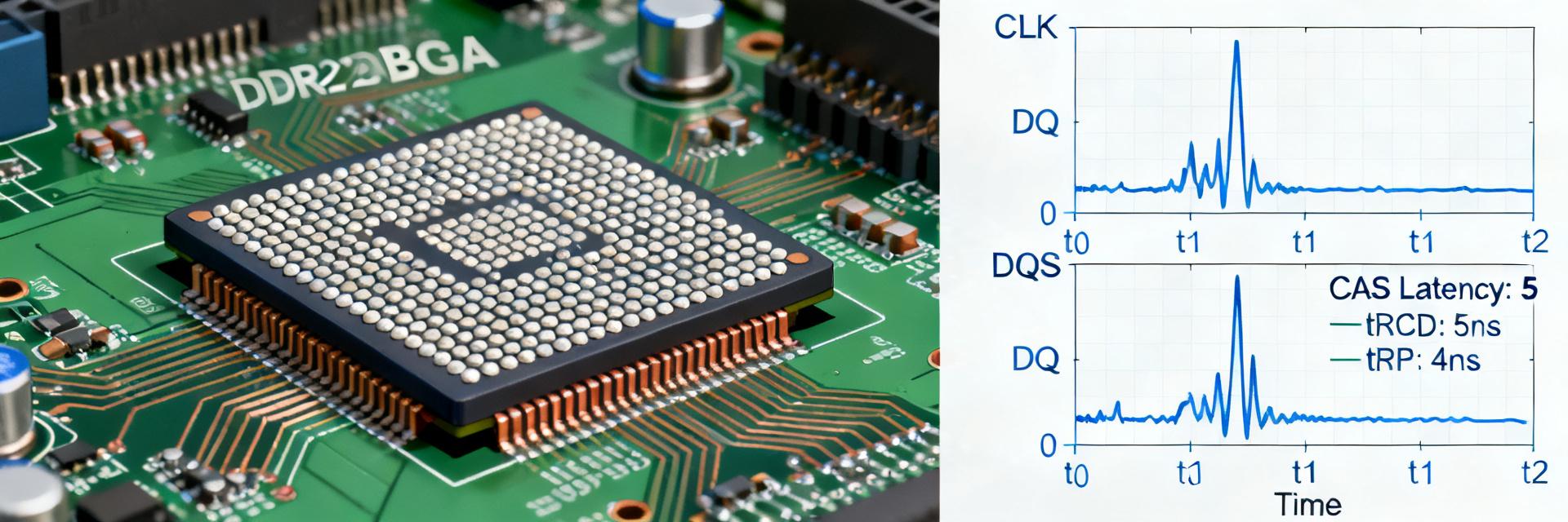
Point: DDR3L nominally operates at 1.35V with standard DDR3 timing parameters directly affecting throughput and latency. Evidence: Speed grades commonly follow MT/s labels such as 1066, 1333, 1600 and 1866, and timing metrics include CAS latency (CL), tRCD, tRP and tRAS on datasheets. Explanation: Lower VDD reduces active and standby power; choose a speed/timing trade-off (lower CL at a given MT/s yields better latency) aligned with controller timing tables and system thermal budget. (Use DDR3L specs from the device datasheet to set controller registers.)
Performance benchmarks & electrical behavior of DDR3L 4Gb (Data analysis)
Throughput, latency and bandwidth across speed grades
Point: Bandwidth scales with MT/s and channel width while latency depends on CAS cycles and tCK; single-rank vs dual-rank affects effective throughput under real workloads. Evidence: A single 64-bit channel at DDR3-1600 (1600 MT/s) yields theoretical peak bandwidth of 12.8 GB/s per channel; rank interleaving and wider channels raise sustained throughput in streaming tests. Explanation: Run sequential and random microbenchmarks to observe how rank count and interleaving impact real-world patterns, and compare latency numbers (ns) by converting CL*tCK for apples-to-apples comparisons.
Power draw and thermal considerations (1.35V benefits)
Point: Operating at 1.35V reduces dynamic power roughly proportional to V^2 and lowers thermal dissipation in tightly packed systems. Evidence: Measured active current decreases when moving from 1.5V to 1.35V; idle power also drops due to lower termination and device standby levels. Explanation: Target VDD/VDDQ measurement points on populated modules during idle and heavy access, and account for Vref stability and board-level heat spread when planning mobile or embedded thermal solutions.
Pinout & package guide for 4Gb DDR3L devices (Method guide)
Common package pinouts: FBGA, TSOP and what to watch for
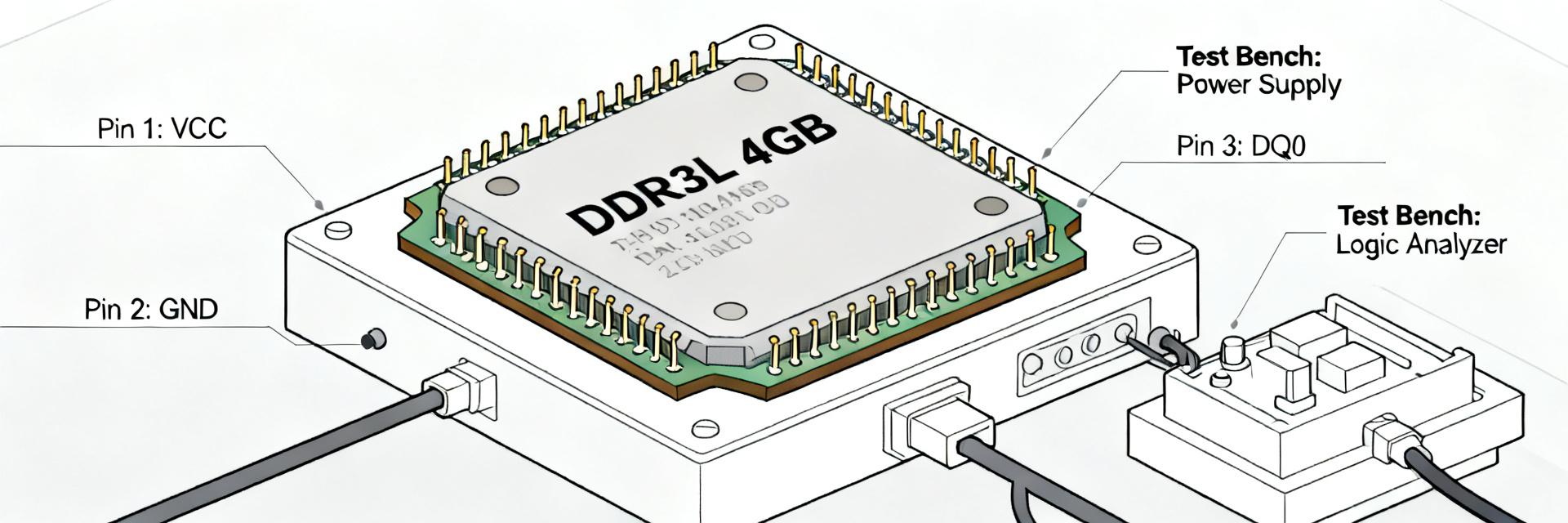
Point: 4Gb DRAM appears in FBGA and TSOP packages with pin assignments for clocks, data strobes and command/address that demand careful layout. Evidence: Datasheet package diagrams identify CK/CK#, DQ/DQS pairs, CA bus, Vref, VDD and VSS locations and recommended decoupling near VDD pins. Explanation: Prioritize matched-length DQ/DQS routing, close decoupling on VDD/VDDQ, and clear return paths for high-speed clocks to preserve signal integrity; consult the device 'pinout' section of the datasheet for exact maps.
SODIMM module pinout notes & mechanical considerations
Point: 204-pin SODIMMs group signals into predictable banks and include mechanical keying that affects module-to-board integration. Evidence: Module drawings lay out signal grouping by pin ranges and specify mechanical dimensions and notch positions for correct seating. Explanation: Route command/address and clock groups with controlled impedance, place termination resistors per reference designs, and account for module height and retention clips when designing chassis and connector placement.
How to pick and validate 4Gb DDR3L parts (Case study / selection)
Reading part identifiers and finding functional equivalents
Point: Part numbers encode density, organization, speed grade, temperature range and package type; equivalence relies on matching key parameters. Evidence: Identifier fields typically include density (4Gb), organization (x4/x8/x16), and speed grade (MT/s) that appear consistently in datasheets. Explanation: For substitutes, verify matching VDD/VDDQ, organization, speed and timing; if rank or width differs, adjust module population or controller configuration accordingly to maintain system compatibility.
Migration compatibility: DDR3 → DDR3L practical checklist
Point: Migrating to 1.35V parts requires platform-level checks for voltage, sequencing and controller support. Evidence: Memory controller manuals and BIOS/firmware tables list supported VDD ranges and timing registers necessary for DDR3L. Explanation: Validate that the SoC/BIOS supports 1.35V operation, confirm power-rail sequencing, and set Vref appropriately; run initial memory training routines and retention tests before production sign-off.
Bench-to-production checklist & troubleshooting (Actionable guidance)
Benchmark setup and validation checklist
Point: A concise validation plan accelerates qualification from lab to production. Evidence: Typical checklists include platform mode (single/dual channel), memory exerciser runs, long-duration stress, and thermal soak tests. Explanation: Capture metrics such as bandwidth, latency, error counts, and VDD/Vref stability; set pass/fail thresholds (no ECC/CRC errors under stress, margin >X%) and document test configurations for repeatability.
Common issues and fixes (signal integrity, timing, Vref)
Point: Frequent failures stem from SI, incorrect timing or Vref miscalibration; targeted diagnostics reveal root causes. Evidence: Symptoms like data-eye closure, command noise, or intermittent bit errors correlate with layout impedance discontinuities and insufficient margin. Explanation: Use scope probing of DQ/DQS, eye-diagram analysis and margin tests; mitigate with proper termination, tightened timing or layout corrections and adjust Vref within datasheet tolerances.
Conclusion / Summary
Point: A disciplined approach to choosing and validating DDR3L parts minimizes risk and shortens time-to-production. Evidence: Focus on density translation, 1.35V electrical requirements and measured benchmark behavior to guide selection. Explanation: Validate pinout and timing early, run the recommended microbenchmarks and margin analyses, and use the bench checklist to confirm parts meet system needs; prioritize pre-production training and thermal verification for successful deployment of DDR3L 4Gb.
Key summary
- DDR3L 4Gb denotes four gigabits per device; use organization (x4/x8/x16) to calculate module capacity and rank topology for controller planning.
- DDR3L specs center on 1.35V operation, speed grades (MT/s) and timing (CL, tRCD, tRP); lower voltage reduces power but requires controller support.
- Pinout attention: prioritize matched DQ/DQS routing, proper decoupling on VDD/VDDQ and correct Vref to maintain signal integrity and timing margins.
Frequently Asked Questions
How do I convert 4Gb device density to a 4GB module?
Point: Conversion depends on device width and number of devices per rank. Evidence: A 4Gb (gigabit) device provides 512MB of capacity if arranged as eight devices of x8 making one 4GB module when populated across ranks. Explanation: Calculate module bytes: (device bits ÷ 8) × number of devices per rank × number of ranks; always confirm organization (x4/x8/x16) in the datasheet before finalizing population.
What tests should I run to validate DDR3L specs on my board?
Point: Run both functional and margin tests to exercise timing and power corners. Evidence: A validation suite should include sequential/random bandwidth, long-duration memory exerciser runs, training repeatability and Vref sweep margin tests. Explanation: Capture bandwidth, latency, error rates and power at idle/active points; document conditions and thresholds to ensure reproducible qualification results.
Can I drop DDR3L into a DDR3 design without changes?
Point: Not always — controller and power must support 1.35V operation. Evidence: Some platforms accept DDR3L in 1.5V-compatible slots, but others require explicit 1.35V support, rail sequencing and BIOS/firmware adjustments. Explanation: Verify controller voltage ranges and training behavior, confirm power-rail sequencing, and perform full system validation to avoid reliability or signaling issues before approving the substitution.
What is the key timing advantage of choosing a lower CL at a given MT/s?
Point: A lower CAS Latency (CL) at a given MT/s yields better overall latency performance. Evidence: Since absolute latency is calculated as CL × tCK, choosing a device with lower clock cycles for column access directly improves data retrieval times in random access scenarios. Explanation: Aligning register configurations with lower cycle latencies lowers system-wide queue overhead, enhancing performance during intensive processor memory bursts.