MT41K256M16TW-107 DDR3L: Complete Specs & Pinout Guide
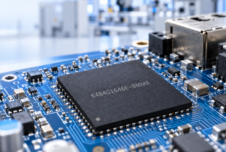
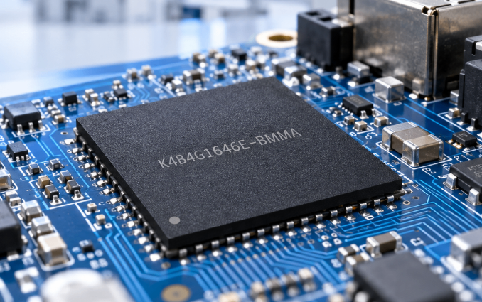
The MT41K256M16TW-107 is a 4 Gbit device organized as 256M × 16 in a 96-ball FBGA, optimized for low-voltage DDR3L operation at 1.35 V and capable of DDR3-1866 timing (effective 933 MHz I/O). These parameters directly affect power budget, board area, and achievable throughput—critical factors for mobile and thermally constrained designs.
This guide delivers a PCB-ready pinout checklist, concise electrical highlights, and practical routing and verification tips designers can apply during schematic capture, layout and lab bring-up without referencing vendor pages—use the official manufacturer datasheet for exact component tables during final sign-off.
1 — Product Overview & Architecture
1.1 — Memory Organization & Capacity
The device presents 4 Gbit total capacity as 256M × 16 data width with internal bank partitioning (multiple banks and selectable bank-address bits). Host controllers see linear addresses mapped to row/column/bank fields; software and memory controller configuration must match the device's row/column sizing to ensure correct addressing and refresh behavior for full capacity utilization.
1.2 — Voltage & Power Modes
Rated for 1.35 V nominal VDD/VDDQ, the part supports standard DDR3L low-voltage operation including active, precharge, and self-refresh low-power states. Using DDR3L reduces DRAM power by tens to hundreds of milliwatts in typical mobile profiles, improving battery life and easing thermal constraints in compact systems compared with traditional 1.5 V DDR3 devices.
2 — Key Electrical Specifications
2.1 — Speed Grades & Timing Parameters
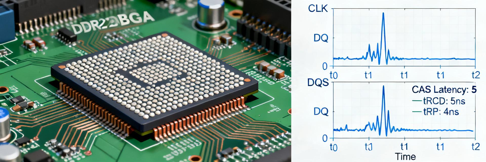
Selected speed grade supports up to a 933 MHz I/O effective rate (DDR3-1866 timing). Designers should reference tCK, CAS latency (CL), tRCD, tRP and tRAS values for the chosen timing point and set controller training margins accordingly. MT41K256M16TW-107 timing choices influence route length budgets and signal integrity requirements on the PCB.
2.2 — Power, Thermal & Reliability Metrics
Typical active and standby currents vary by access pattern; expect higher VDD/VDDQ currents during sustained reads/writes and much lower currents in self-refresh. Design PDN to handle peak active currents plus margin, monitor die temperature with thermals on critical boards, and verify JEDEC-compatible reliability parameters using the manufacturer datasheet before final approval.
| Parameter | Representative value |
|---|---|
| Density / Organization | 4 Gbit (256M × 16) |
| Nominal VDD / VDDQ | 1.35 V (DDR3L) |
| Max I/O rate | 933 MHz effective (DDR3-1866 timing) |
3 — Pinout & Package Details
3.1 — Package Type, Ball Count & Mechanical Notes
The part comes in a 96-ball TFBGA/FBGA package with a tight ball pitch and compact footprint; follow the recommended land pattern from the official mechanical drawing during PCB library creation. Pay attention to reflow profile recommendations and handling notes to prevent warpage; include a properly dimensioned courtyard and thermal vias if the datasheet suggests a center expose pad.
3.2 — Signal Groups & Ball Mapping
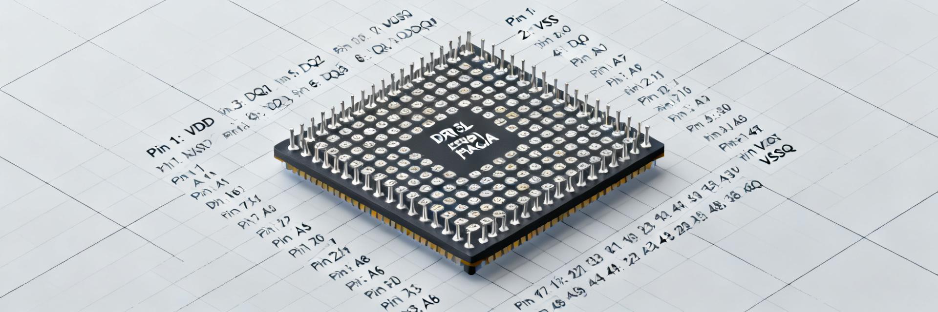
Group and label power clusters (VDD/VSS), DQ[0:15] and associated DQS/DQS# strobes, address lines A[0:N], bank address BA0–BA2, command pins RAS/CAS/WE, differential clocks CK/CK#, CKE, ODT, RESET#, and VREF. The pinout schematic map is represented in the diagram below to aid accessibility and layout capture.
4 — Timing, Signal Integrity & Routing Guidelines
4.1 — Clocking, Termination & Impedance Control
Route CK/CK# as tight differential pairs with controlled 100 Ω differential or 50 Ω single-ended reference impedance per board stack-up. Use manufacturer-recommended RTT termination settings implemented near the controller or the DRAM as appropriate; place VREF decoupling next to VREF ball clusters to stabilize reference for on-die termination behavior.
4.2 — Data Strobe, Fly-by Topology & Length Matching
Implement fly-by topology for address/command with series termination at the controller and short stub connections to each rank. For DQ/DQS use source-synchronous routing with DQS capture timing in mind—match DQ-to-DQS within each byte lane and keep skew budgets tight; limit stub lengths and adhere to the controller's recommended maximum trace lengths.
5 — PCB Integration Checklist & Example Schematic Notes
5.1 — Power Delivery & Decoupling Strategy
Place high-frequency decoupling capacitors (0.01–0.1 μF) and bulk caps near VDD and VDDQ ball groups; follow the datasheet suggested capacitor mix and place them on the component side within a few millimeters of the balls. Verify PDN with impedance targets and run power sequencing checks to respect VDD/VDDQ ramp order during bring-up.
5.2 — Example BOM, Layout Tips & Verification Steps
Typical BOM includes appropriate capacitor values, small series resistors for data lines if required, and 0 Ω or ferrite for power routing. Layout guidance: keep command/address runs short and straight, cluster decoupling near the device, and place termination near the source. Verify with IBIS/SPICE models and run DDR training and margin tests in the lab.
6 — Common Issues, Troubleshooting & FAQs
6.1 — Typical Failure Modes & Diagnostic Flow
Common failures: training failures, marginal eye due to SI, incorrect VREF or RTT settings, and address parity errors. Triage by first validating power rails and VREF, then capturing clock and data with a high-speed scope during DDR training. Progress to controlled timing sweeps and termination adjustments to isolate root causes quickly.
6.2 — Quick FAQ & Selection Advice
Choose x16 when system bus efficiency and higher width matter; x8 parts provide routing flexibility for multi-rank configurations. Single-rank designs simplify timing and routing; multi-rank increases capacity but tightens signal integrity constraints. Compare density, voltage, and package footprint to match your board's PDN and thermal budgets.
Summary
The device offers 4 Gbit capacity arranged as 256M × 16 with low-voltage DDR3L operation at 1.35 V, and requires disciplined pinout, termination and routing practices to achieve reliable DDR3-1866 performance. Prioritize correct VREF/RTT settings, clustered decoupling, and byte-lane length matching for a predictable bring-up. Reference the official datasheet and pinout PDF early and execute the verification checklist before tape-out.
Key Takeaways
- MT41K256M16TW-107 provides compact 4 Gbit DDR3L density useful for space-constrained designs; verify addressing and controller settings to map the 256M × 16 organization correctly.
- Low-voltage DDR3L (1.35 V) reduces power and thermal load; implement recommended PDN decoupling and monitor VDD/VDDQ during active workloads.
- Pinout and routing priorities: group power pins, stabilize VREF, route CK/CK# as controlled differential pairs, and match DQ/DQS lengths per byte lane for robust signal integrity.
Frequently Asked Questions
Is MT41K256M16TW-107 suitable for low-power mobile applications?
Yes—its DDR3L 1.35 V operation lowers active and standby power relative to 1.5 V parts. Combine careful PDN design and appropriate low-power modes (self-refresh during suspend) to maximize battery life; validate idle and active current in a representative system to confirm expected savings.
What are the most important pinout considerations for layout?
Prioritize grouping VDD/VSS clusters and placing decoupling close to power balls, mark NC/test balls clearly, provide a solid reference plane under CK/CK#, and annotate DQ/DQS pairs in the pinout so layout engineers can enforce byte-lane matching and keep stubs minimal for reliable timing margins.
Which lab checks should be performed after layout to validate DDR3L integration?
Run DDR controller training, capture eye diagrams on read/write operations, sweep address/command timing margins, validate VREF and termination settings, and perform write/read margin tests across temperature and voltage corners. Use IBIS/SPICE simulations and real silicon training logs to iterate until margins meet target specifications.
What is the significance of the DDR3-1866 speed grade for this device?
The DDR3-1866 timing capability supports up to a 933 MHz I/O clock (1866 MT/s effective data rate). This high-speed performance requires precise trace length matching, strict 50-ohm single-ended / 100-ohm differential impedance control, and optimized ODT settings to ensure clean signal transitions and adequate margin.