MT62F1G32D2DS-023 LPDDR5X Specs: Complete Datasheet Overview
This guide unpacks the MT62F1G32D2DS-023 LPDDR5X datasheet and translates the key electrical, timing, package, and integration specs engineers need to design with this 32Gb-class LPDDR5X device. Point: Present headline numbers up front; Evidence: Datasheet tables list 32Gb density and high-bandwidth speed grades; Explanation: Readers can map those numbers to system bandwidth and integration risk quickly.
Point: Article structure and reading order are pragmatic for bring-up. Evidence: The following sections move from device overview to electrical, performance, package, then a hands-on checklist. Explanation: Recommended reading order is Introduction → Device overview → Electrical/timing → Integration/performance → Package/thermal → Design checklist → Summary and FAQ for fast design-review use.
Device overview & key features
Part numbers, density & speed grades
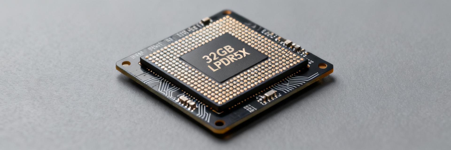
Point: The device family covers a 32Gb density (4GB-equivalent) in x32 organization. Evidence: The datasheet part mapping table lists suffix variants tied to speed grades. Explanation: Use the table below to match suffix → density → peak data rate when choosing parts and listing long-tail keywords for procurement and BOM notes.
| Part suffix | Density | Max data rate (Mb/s per pin) |
|---|---|---|
| -023 | 32Gb (4GB equiv.) | 8533 |
| -WT | 32Gb (4GB equiv.) | 7400 |
Core device features & standards support
Point: Primary features include x32 bus, multi-bank architecture, low-power modes, and optional on-die features. Evidence: Datasheet feature checklist enumerates channel width, bank count, LPDDR5X low-power states, and training support. Explanation: Confirm JEDEC compliance rows and optional items (on-die ECC, enhanced training) in the datasheet to validate controller compatibility early.
Electrical characteristics & timing
Supply voltages, IO specs & power modes
Point: Nominal core and I/O voltages and power-state currents drive decoupling and power-sequencing decisions. Evidence: The datasheet voltage tables list VDD, VDDQ ranges and dynamic/static current at defined data rates. Explanation: Use those table values to size regulators, place decoupling near VDD/VDDQ pins, and plan power sequencing with recommended topologies to limit inrush and droop.
Timing parameters, data rates & bandwidth
Point: Timing metrics (tCK, tRCD, CAS-like latencies) determine controller setup. Evidence: Timing tables provide tCK ranges and timing rows per speed grade; max listed data rate yields raw bandwidth. Explanation: Convert listed data rate to peak bandwidth by: bandwidth = data rate × bus width / 8. For x32 at 8533 Mb/s, peak ≈ 34.1 GB/s per device.
Performance & system integration
Calculating effective throughput & latency trade-offs
Point: Theoretical peak differs from sustained throughput due to refresh, conflicts, and bursts. Evidence: Datasheet rates and timing rows define theoretical max; system-level models show refresh/row-hit effects. Explanation: Run sample calculations combining device peak bandwidth, x32 width, and realistic duty factors (for example 60–80% sustained) to size memory paths and expected latency.
Controller/PHY configuration and signal integrity checklist
Point: Correct PHY setup and SI practices prevent training failures. Evidence: Datasheet notes cover WCK/CK ratios, required training sequences and ODT recommendations. Explanation: Verify WCK/CK mode, training step ordering, termination values, impedance targets, and trace length matching during schematic and PCB review before first power-up to reduce bring-up iterations.
Package, thermal & reliability considerations
Package details, pinout & footprint guidance
Point: The device uses a high-ball-count BGA-style package with tight land-pattern tolerances. Evidence: Mechanical drawings and pinout tables in the datasheet specify ball map and keepout dimensions. Explanation: Extract critical dimension rows, verify land pattern, and prioritize routing for power/ground, clocks and command/address lanes while reserving keepout areas for thermal vias.
Thermal limits, operating ranges & qualification notes
Point: Operating temperature and junction limits set derating and thermal mitigation needs. Evidence: The datasheet lists operating temperature ranges, Tmax junction and recommended thermal suggestions. Explanation: Derive PCB copper, thermal via arrays and possible heatsinking from those numbers and confirm qualification (JEDEC/AEC notes) for your target application and environmental tests.
Design checklist & practical validation steps
Schematic, power sequencing & PCB routing checklist
Point: A prioritized checklist prevents common schematic/PCB errors. Evidence: Datasheet sections define recommended sequencing, decoupling placement and WCK/CK routing. Explanation: Enforce power order, place decoupling within millimeters of VDD pins, use star routing for supplies, match WCK/CK pairs, and validate ODT and termination values in schematic notes before layout sign-off.
Firmware/bring-up & validation plan
Point: A staged bring-up plan reduces risk and isolates faults. Evidence: Protocol training flow and PHY calibration sequences are described in the datasheet training notes. Explanation: Begin with power and continuity checks, then run JEDEC training, PHY calibration, stress patterns and timing margin sweeps; collect pass/fail criteria for latency, throughput and bit-error-rate under thermal stress.
Summary - Key takeaways
- Confirm part-suffix to density and speed mapping from the datasheet before BOM freeze; this ensures correct MT62F1G32D2DS-023 speed grade selection and controller timing targeting.
- Size regulators and decoupling from the listed VDD/VDDQ ranges and dynamic/static currents; place decoupling close to power pins and plan power sequencing per datasheet notes.
- Convert listed data rate to peak bandwidth with bandwidth = rate × bus width ÷ 8 and plan sustained throughput at 60–80% of peak to account for refresh and bank conflicts.
Frequently Asked Questions
What are the essential voltage ranges in the MT62F1G32D2DS-023 LPDDR5X datasheet?
Point: Knowing nominal and allowable voltage ranges avoids damage and timing shifts. Evidence: Voltage tables specify VDD and VDDQ nominal and min/max limits. Explanation: Use those ranges to pick regulators with margin, implement power sequencing rules, and verify decoupling to keep transient excursions within specified limits during high-rate transfers.
How do I convert the datasheet data rate to system GB/s for x32 devices?
Point: Conversion is straightforward and critical for bandwidth budgeting. Evidence: The datasheet lists max data rate in Mb/s per pin for each speed grade. Explanation: Apply bandwidth = data rate × 32 ÷ 8; for an 8533 Mb/s grade the peak device bandwidth ≈ 34.1 GB/s, then factor realistic duty cycle for sustained throughput.
Which checklist items in the datasheet are most often missed during bring-up?
Point: Common misses are sequencing, termination and training order. Evidence: Datasheet recommended sequencing, ODT notes and training steps are explicit. Explanation: Double-check power-up order, ODT and termination values, WCK/CK routing and length matching, then run the prescribed training sequences immediately after powering to avoid elusive timing and SI failures.
What are the primary differences between the -023 and -WT speed grades?
Point: The main distinction lies in maximum bandwidth performance parameters. Evidence: The speed grade lookup tables in the datasheet map -023 to a peak of 8533 Mb/s per pin and -WT to 7400 Mb/s per pin. Explanation: Design engineers should utilize the -023 speed grade when designing for peak performance applications and the -WT speed grade for mainstream bandwidth layouts.