MT25QL256ABA8E12-1SIT Datasheet: Key Specs & Pinout
The MT25QL256ABA8E12-1SIT is a 256‑Mbit serial NOR flash device with high‑speed I/O, commonly rated for up to 133 MHz clock operation; this combination makes it a frequent choice for firmware storage and boot ROM in embedded systems. This article gives you a concise reference of key specs, full pinout guidance, interface tips, and a practical implementation checklist—consult the official datasheet for absolute values and revision details.
You will find focused sections: background and typical uses, electrical and performance highlights, a clear pinout table, interface/command guidance, plus PCB layout and debug steps. Treat the manufacturer datasheet as the source of truth for precise timing, current values, and package drawings before production or qualification.
1 — Background: What the MT25QL256ABA8E12-1SIT Is
1.1 Device class & common applications
Point: This part is a serial NOR flash memory device that supports SPI and higher‑I/O modes.
Evidence: The device class and quad I/O capability are documented in the official materials.
Explanation: You’ll typically use it for firmware and boot storage, LUTs, configuration blobs, and small file systems in IoT, consumer electronics, and embedded controllers where random‑read and execute‑in‑place are valuable.
1.2 How to use the datasheet as source of truth
Point: The datasheet is the authoritative reference for electrical, timing, pin descriptions and mechanical drawings.
Evidence: Key sections to prioritize are electrical characteristics, pin descriptions, timing diagrams, and the command set.
Explanation: When you quote voltages, currents, or opcodes for production, cross‑check revision numbers and page figures in the official datasheet to avoid mistakes in implementation and procurement.
2 — Key Electrical & Performance Specs
| Parameter / Feature | Specification Details |
|---|---|
| Memory Capacity | 256 Megabit (32 Megabytes) |
| Supply Voltage (VCC) | 1.7V to 2.0V Range (1.8V Nominal) |
| Max Clock Frequency | Up to 133 MHz (Single / Quad I/O Modes) |
| Erase Granularity | 4KB Subsector, 64KB Sector, Bulk Erase |
| Data Retention | 20 Years (Typical at System Operating Temperature) |
2.1 Memory organization, capacity, and endurance
Point: The device provides 256 Mbit total capacity organized into bytes and conventional pages and blocks.
Evidence: The datasheet lists total bits/bytes, page sizes, sector/block erase granularity, program/erase endurance cycles, and data retention guarantees.
Explanation: For example, you should map firmware images to page and sector boundaries, plan erase cycles per block within endurance limits, and confirm retention specs for your product lifetime.
2.2 Power, timing, and performance highlights
Point: Expect a specified VCC range, operating currents for read/program/erase, and a maximum clock near 133 MHz.
Evidence: Datasheet tables differentiate typical vs. max currents, list I/O timing parameters (tCH, tCL, tCS), and note different values for STR, DTR or quad modes.
Explanation: Use the compact timing table for clocking decisions, and plan for low‑power standby values and any mode‑specific current increases during program/erase.
3 — Pinout & Package Details
3.1 Pin mapping: functional pin table
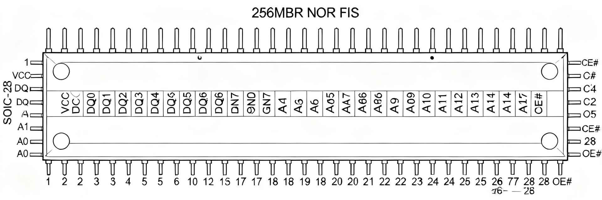
Point: The pinout assigns pins for IO0–IO3, SCK, CS#, power and ground; some pins are active‑low control signals.
Evidence: Typical functional names include IO0 (SI), IO1 (SO), SCK (clock), CS# (chip select), WP# (write protect) and HOLD#; power pins carry VCC and multiple GND pins for thermal/current return.
Explanation: Review the pinout table carefully to wire CS#, WP# and HOLD# correctly, tie unused inputs per the datasheet, and respect IO voltage domains to avoid latch‑ups.
3.2 Package drawing, footprint and mechanical notes
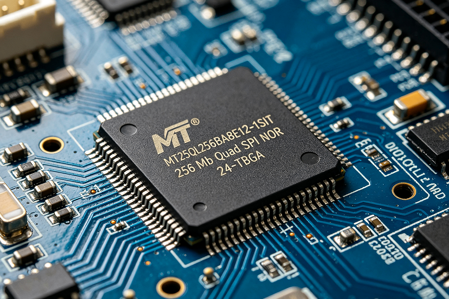
Point: Multiple package variants and mechanical dimensions are provided; footprint guidance is critical.
Evidence: Mechanical drawings specify pad layout, recommended solder mask openings, pad dimensions, pin‑1 indicator and board keepouts.
Explanation: When you design the footprint, follow the recommended pad sizes, add solder mask clearance, mark pin‑1, and include thermal/ground vias as advised to ensure solderability and thermal performance.
4 — Interface Modes, Commands & Timing Diagrams
4.1 SPI / Quad I/O modes and common commands
Point: The device supports single‑SPI and multi‑I/O modes and a compact command set for read, program, erase and status operations.
Evidence: Common opcodes include Read (and Fast Read variants), Page Program, Sector/Block Erase, Read ID, Write Enable/Disable, and Reset.
Explanation: In practice, implement a minimal command subset for bring‑up (Read ID, Read, Write Enable, Page Program, Erase), and consult the datasheet opcode map for full command lengths and expected response bytes.
4.2 Timing diagrams and example sequences
Point: Key sequences are read, page program and erase flows with CS# toggling and address phases.
Evidence: Timing diagrams in the datasheet show clock polarity/phase, command/address/data windows, and required delays between operations.
Explanation: A typical sequence is CS# low → opcode + address → data transfer → CS# high; use the specified clock phase/polarity and required inter‑command delays, and capture signals with a logic analyzer to validate timing during bring‑up.
5 — Design, Layout & Debug Checklist
5.1 PCB layout and power sequencing best practices
Point: Proper decoupling, short clocks, and clean ground routing directly affect reliability.
Evidence: Recommended practices include placing decoupling caps close to VCC pins, using star or plane grounds, and routing clock/IO traces short with series damping resistors if needed.
Explanation: Place 0.1 μF and 1 μF decouplers near power pins, avoid long stub traces to the flash, and consider level shifters if the host MCU I/O voltage differs from the flash VCC.
5.2 Common failure modes and troubleshooting steps
Point: Many failures stem from wiring, power, or timing mismatches.
Evidence: Typical issues are incorrect pin mapping, missing decoupling, SPI mode mismatch, floating HOLD/WP, or signal integrity artifacts.
Explanation: For debug, verify VCC and GND, toggle CS while capturing the bus with a logic analyzer, issue a Read ID as the first test, and inspect solder joints and footprint alignment if communication fails.
Summary
- The MT25QL256ABA8E12-1SIT is a 256‑Mbit serial NOR flash suited for firmware and boot storage; consult the official datasheet for exact capacity, endurance and timing before production.
- Key electrical items: check VCC range, active/read/program currents, and max clock (near 133 MHz); align your firmware image to page/sector sizes listed in the datasheet.
- Use the pinout and package guidance when placing the footprint: follow pad sizes, pin‑1 marking, decoupling placement, and ground/thermal recommendations to avoid assembly and reliability issues.
6 — Common Questions
What are the essential steps to validate MT25QL256ABA8E12-1SIT on a new board?
Start by checking power rails and decoupling, confirm correct footprint and pin mapping, then issue a Read JEDEC/ID command with the chip selected. Use a logic analyzer to capture clock and IO lines; successful ID response and stable read transactions confirm basic communication before programming tests.
How do you choose the right SPI mode and clock settings for MT25QL256ABA8E12-1SIT?
Refer to the timing diagrams for required clock polarity and phase; begin with a conservative clock (e.g., a fraction of max) to validate signal integrity. Gradually increase clock to the device’s supported maximum while monitoring for CRC or read errors; select STR/DTR or Quad modes only after verifying electrical margins.
What are the quickest troubleshooting steps when MT25QL256ABA8E12-1SIT fails to respond?
Verify VCC/GND voltages, ensure CS# is asserted correctly, check HOLD#/WP# states, inspect solder joints, and capture SPI traffic. If you see no activity, reflow or check footprint alignment; if traffic is noisy, add series resistors and shorten traces. Finally, attempt a Read ID as an initial sanity check.
How should the WP# and HOLD# pins be handled if they are not actively used?
If WP# (Write Protect) and HOLD# (Hold) functions are not actively controlled by the host MCU, they should be pulled high to VCC through individual pull-up resistors (typically 4.7kΩ to 10kΩ). Leaving these inputs floating can lead to accidental write-protection or clock suspension, causing unpredictable device behavior.