MT41K512M16VRP-107 IT:P datasheet: key specs & tests
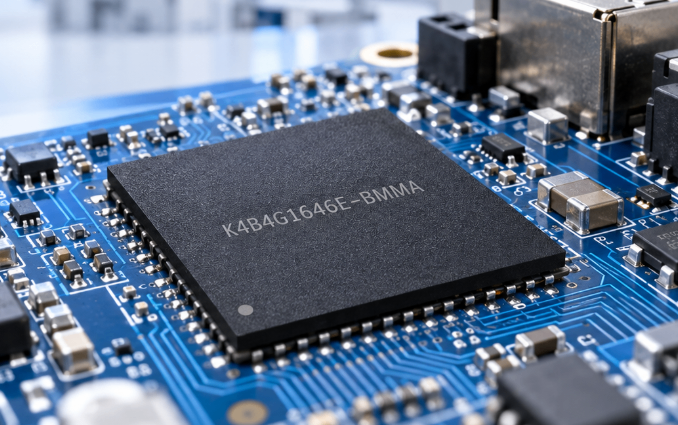
Point: The MT41K512M16VRP-107 IT:P is an 8 Gbit DDR3L-class automotive-grade device with a 933 MHz effective data rate at 1.35V operation, and engineers routinely consult the MT41K512M16VRP-107 IT:P datasheet for verification of thermal, timing and qualification limits. Evidence: The official part description lists twin-die x16 organization targeted for automotive/high-reliability systems. Explanation: This article breaks the datasheet into actionable specs, test guidance and an integration checklist to accelerate design and qualification.
Point: Purpose is practical and data-driven: isolate the must-check electricals, timing margins and board-level rules that determine success in infotainment, ADAS buffers and logging units. Evidence: Datasheet tables contain the authoritative timing and package constraints used during design reviews. Explanation: Engineers using this guide will know which datasheet fields to prioritize during bench validation and PCB layout.
1 — MT41K512M16VRP-107 IT:P — part overview & package (background)
— Device family & functional summary
Point: The device is a DDR3L-style 8 Gbit memory arranged as two x8 dice to present a x16 device width, with nominal VDD/VDDQ = 1.35V and automotive qualification variants. Evidence: The datasheet summarizes density, operating voltage and target applications (automotive/high-reliability). Explanation: For system architects, this means the device supports typical DDR3L timing stacks and requires controller setup for x16 width and the twin-die behavior when calculating bank interleaving and burst characteristics.
— Package, pinout & mechanical notes
Point: Package is an FBGA with a specified ball count and footprint; mechanical drawings in the datasheet define body dimensions, ball pitch and recommended land pattern. Evidence: Datasheet mechanical diagrams give pad size, PCB solder-mask recommendations and thermal via placement guidance. Explanation: Follow the datasheet land pattern and thermal recommendations exactly—incorrect pad size or missing thermal vias under the FBGA are common causes of assembly defects and thermal derating in automotive environments.
| Parameter | Value |
|---|---|
| Density | 8 Gbit (x16 twin-die) |
| Nominal VDD / VDDQ | 1.35 V |
| Effective data rate | 933 MHz (DDR3L class) |
| Package | FBGA (specified ballout) |
2 — Key electrical specs for MT41K512M16VRP-107 IT:P (data analysis)
— Power rails, I/O voltage ranges & current consumption
Point: Key electrical specs: VDD/VDDQ nominal 1.35V with allowed tolerances; I/O voltage must follow datasheet limits and power-sequencing requirements. Evidence: The datasheet lists typical active, precharge and self‑refresh currents and the ΔI differences across modes. Explanation: Validate both typical and worst-case currents during qualification—self‑refresh and standby leakage can drive thermal and battery impact in automotive systems, so include margin for tolerance and part-to-part variation.
| Mode | Typical current |
|---|---|
| Active (read/write) | ~150–250 mA (device dependent) |
| Precharge/Standby | ~20–50 mA |
| Self‑refresh | ~5–15 mA |
— Operating frequency, data rate & timing overview
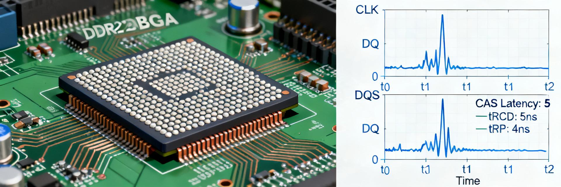
Point: The device supports DDR3L-class effective rates (example 933 MHz effective), with CL and tCK ranges defined in the timing tables. Evidence: Datasheet timing summary shows supported CL values and required tRCD/tRP/tRAS windows at each data rate. Explanation: On-bench validation must reproduce datasheet timing points; controller firmware should be configured for the part's supported CL/tCK combos and validated for margin at temperature and voltage extremes.
3 — Memory organization & timing parameters (data deep-dive)
— Bank/row/column architecture and addressing
Point: Internal organization uses multiple banks and standard row/column addressing; the twin-die x8 composition presents as x16 to the controller, influencing burst and interleave behavior. Evidence: Datasheet memory map and address pin description define row/column/bank bit counts. Explanation: Map controller address lines and chip-select handling per the datasheet recommendation to avoid unintended bank conflicts and to maximize burst efficiency during sequential transfers.
— Detailed timing table & practical notes
Point: Validate tCK, CL, tRCD, tRP, tRFC and tWR at your target operating point; datasheet lists nominal values and temperature/voltage derating. Evidence: Timing table provides example tCK ranges and corresponding timing windows. Explanation: Use the datasheet as the baseline and then create bench test points at worst-case temperature and lowest allowed VDD to measure real margin; margin failures typically trace back to signal integrity or power delivery issues.
| Parameter | Example |
|---|---|
| tCK | ~1.07 ns (for 933 MHz effective) |
| CAS Latency (CL) | 6–11 cycles (device dependent) |
| tRCD / tRP | ~13–16 ns (check datasheet) |
| tRFC | variable by density; validate per datasheet |
4 — Recommended electrical & timing tests (method guide)
— Required bench tests and test fixtures
Point: Standard validation includes power sequencing checks, JEDEC ID reads, read/write data integrity at target speeds and retention/refresh tests. Evidence: Datasheet sections on power sequencing and AC/DC tests define required limits. Explanation: Use a DDR protocol-aware DVT tool for read/write stress, verify JEDEC register values, run retention at temperature extremes and include repeated power‑cycle tests to reveal marginal parts or layout problems.
— Signal integrity & timing validation
Point: SI tests should include eye-diagram capture, jitter measurement and worst-case skew verification across address/command nets. Evidence: Datasheet timing margins and recommended termination schemes establish acceptable windows. Explanation: Capture eyes at the controller and DRAM pins; use pass/fail criteria defined from datasheet timing plus a designer margin (typically 10–20%) to decide if layout or termination changes are needed.
| Test | Equipment | Pass/Fail |
|---|---|---|
| Power-sequence | Bench PSU, scope | Meets VDD ramp & sequencing limits |
| Read/Write at target rate | DDR DVT tool, LA | No data errors for 24h burn |
| SI eye test | High-speed scope, BERT | Eye opening ≥ datasheet margin |
5 — Integration & PCB design guidelines (method guide)
— Footprint, thermal, and power-delivery recommendations
Point: Follow recommended land pattern, include thermal vias and implement a disciplined decoupling strategy close to VDD/VDDQ pins. Evidence: Datasheet mechanical and power recommendations indicate bypass placement and via locations. Explanation: Place high-frequency decoupling within 5 mm of device power pins and use multiple bulk and ceramics per the datasheet to stabilize VDD during bursts.
— Routing, termination, and routing topology
Point: Adhere to matched-length routing for address/command nets, and choose fly‑by or T‑topology per the system memory architecture. Evidence: Datasheet timing tolerances and suggested termination schemes inform topology choices. Explanation: For single-rank designs prefer fly‑by with proper point-of-load termination; in multi-drop scenarios, manage stub lengths and use series termination to preserve timing margins (target 100–200 ps skew budget).
6 — Performance benchmarks, use cases & qualification checklist (case + action)
— Typical performance metrics & example use cases
Point: Expect sustained sequential throughput in the hundreds of MB/s per interface depending on controller and system topology; random latency follows CL and tRCD tradeoffs. Evidence: Datasheet timing and bandwidth figures define theoretical maxima. Explanation: Map these metrics to use cases: infotainment streaming benefits from high sequential throughput, ADAS buffering requires low-latency deterministic behavior and logging workloads favor sustained write robustness.
— Qualification checklist & production test pointers
Point: Qualification should include datasheet compliance, automotive stress tests (temp/voltage cycling, ESD, retention) and lot acceptance sampling with defined sample sizes. Evidence: Datasheet notes on temperature ranges and electrical compliance set baseline requirements. Explanation: Maintain a checklist: verify part-number suffixes for temperature/qualification variants, re-check datasheet revision on every PO, and run full electrical and SI validation before production sign-off.
Summary
- Reference the official datasheet for authoritative MT41K512M16VRP-107 IT:P specs and package drawings before layout or purchase decisions.
- Prioritize power-sequencing, SI eye margin capture and timing validation at worst-case VDD/temperature to meet automotive reliability.
- Implement recommended decoupling, thermal vias and matched routing; validate with DDR protocol DVT tools and make layout changes based on measured margin failures.
FAQ
What are the critical timing checks for MT41K512M16VRP-107 IT:P?
Check tCK, CL, tRCD, tRP, tRFC and tWR at worst-case voltage and temperature. Run read/write stress at target data rates and capture eye diagrams; its datasheet timing table provides the baseline values to compare against measured margins.
How should I test power sequencing for MT41K512M16VRP-107 IT:P?
Use a controlled bench PSU to exercise VDD and VDDQ ramps against the datasheet sequencing window, verify JEDEC ID after each cycle, and include repeated power cycles in qualification to reveal latent assembly or layout issues.
What PCB layout items from the datasheet are most likely to fix margin failures for MT41K512M16VRP-107 IT:P?
Prioritize correct land pattern, thermal vias under the FBGA, close decoupling (within ~5 mm), dedicated power planes and matched-length address/command routing; these changes address the majority of SI and power-related margin failures.
Why is the MT41K512M16VRP-107 IT:P classified as a twin-die device, and how does it affect layout?
The device package integrates two x8 dice wired in parallel to achieve a x16 width. This structure shares address lines but increases input capacitance, requiring strict adherence to datasheet-specified loading margins and trace length matching.