K4B4G1646E-BYMA Technical Datasheet: Full Pinout & Timing
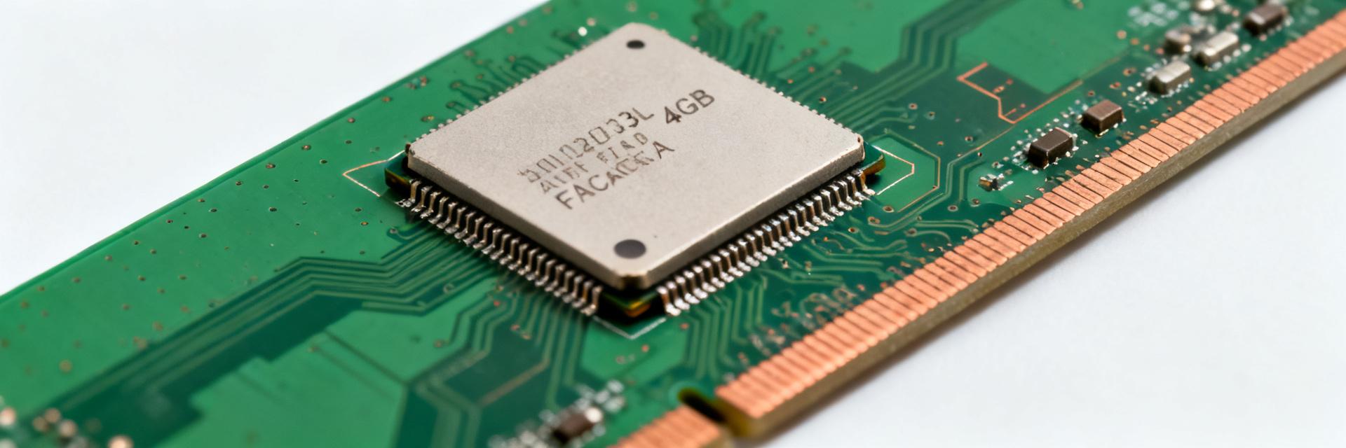
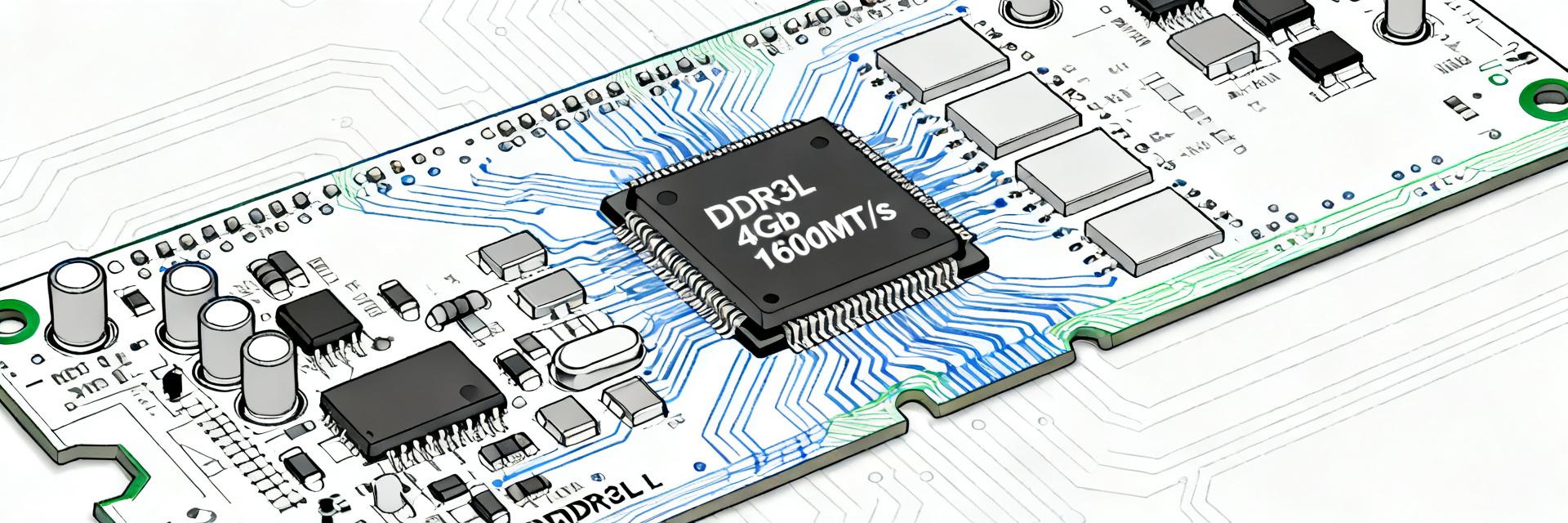
The K4B4G1646E-BYMA is a high-performance 4Gb DDR3L SDRAM component engineered specifically for low-voltage, high-density system memory architectures. Representing a 256M x16 configuration, this device runs at a nominal 1.35V operational supply, housed within a compact 96-ball FBGA package. Supporting interface speeds up to approximately 933 MHz (DDR3-1866 speed bin), this technical reference synthesizes critical electrical, layout, and timing guidelines to ensure robust design bring-up and physical layer validation.
This document distills critical reference metrics from the DDR3L specification into an actionable design guide focusing on timing budgets, ballout grouping, physical layout constraints, and standard validation sequences for FAEs, PCB designers, and signal integrity engineers.
1 — Background & Key Specifications
1.1 — Part Summary & Target Applications
Point: The K4B4G1646E-BYMA provides 4Gb density organized in a x16 parallel interface configuration, prioritizing high-bandwidth data transfers in a space-constrained form factor.
Evidence: Standard JEDEC specifications register this device within the 96-ball FBGA footprint, utilizing an optimized 1.35V supply while maintaining backward compatibility with 1.5V signaling networks.
Explanation: This component is ideally suited for modern embedded architectures, networking platforms, and industrial systems where high-frequency throughput, low standby currents, and compact footprint parameters are mandatory design constraints.
1.2 — Modes of Operation & Variants to Watch
Point: The memory array interfaces via flexible JEDEC configurations including DLL enable/disable options, dynamic On-Die Termination (ODT), and write leveling calibration.
Evidence: System configuration relies on four internal Mode Registers (MR0–MR3) that program operation modes and address decoding pathways.
Explanation: Hardware and firmware development teams must guarantee precise controller configuration of initialization sequences and timing margins to prevent physical bus contention and initialization lockups.
2 — Full Pinout Breakdown
2.1 — Ball/PIN Map & Grouping
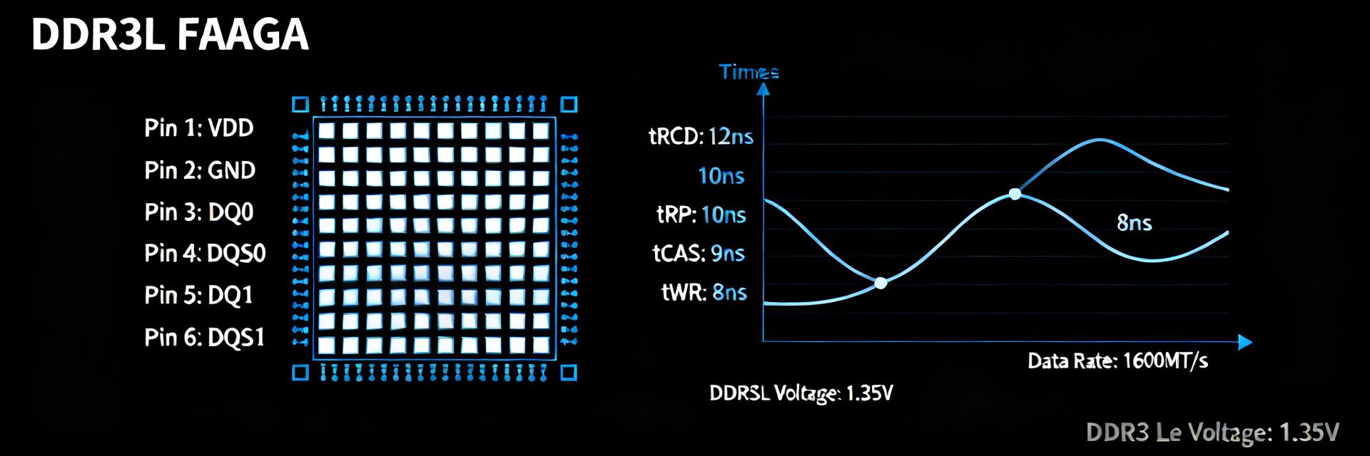
Point: The 96-ball layout segregates system buses into dedicated geographic zones to minimize signal cross-coupling and facilitate clean routing topologies.
Evidence: The interface grouping maps the byte lanes (DQ0–DQ7 and DQ8–DQ15) with their associated lower and upper strobes (LDQS/UDQS), isolating them from the command/address bus.
| Ball Group | Function | Key Notes |
|---|---|---|
| ADDR / CTRL | A0–A14, BA0–BA2, RAS#, CAS#, WE# | A12/BC# (Burst Chop), A10/AP (Auto-Precharge) |
| CK / CK# | Differential Clock Inputs | Must be routed as differential pairs with matched impedance |
| DQ / DQS | DQ0–DQ15, LDQS, LDQS#, UDQS, UDQS# | Matched-length trace grouping required per byte lane |
| VDD / VSS | Power and Ground Supply Lines | Requires dedicated decoupling loops and low-impedance planes |
2.2 — Power Rails, Decoupling & Thermal Pads
Point: Correct power delivery network (PDN) decoupling design is critical to avoid voltage drop (IR-drop) during concurrent memory operations.
Evidence: Specifications dictate distinct VDD (core voltage) and VDDQ (I/O driver supply) inputs, supplemented by an analog VREF reference line.
Explanation: High-frequency ceramic capacitors must reside immediately adjacent to the FBGA power vias. Designers must isolate VREFDQ and VREFCA lines from high-speed digital switching fields to prevent noise-induced signal jitter.
3 — Timing Parameters Explained
3.1 — Core Timing Glossary
Understanding and calculating timing boundaries ensures high-speed signals settle before evaluation cycles:
- tCK (Clock Cycle Time): Specifies the minimum operational clock period (e.g., ~1.07ns for DDR3-1866).
- tRCD (RAS to CAS Delay): Internal command interval between active bank command and read/write column access.
- tRP (Row Precharge Time): Delay constraint to close and precharge an open memory row.
- tRAS (Active to Precharge Delay): Minimum time to keep a row active before executing precharge routines.
- CL (CAS Latency): Clock cycles separating the read command receipt from the first output data element.
3.2 — Calculating Timing Margins
Point: Absolute clock metrics must account for dynamic operational shifts caused by temperature, voltage fluctuations, and layout skew.
Evidence: At 933 MHz (tCK = 1.07 ns), minor layout variations can consume a significant fraction of the unit interval (UI).
Explanation: Signal simulation tools must include the physical trace-length delay plus internal silicon propagation delay. Designing with a robust 10–20% margin ensures reliable high-speed data sampling across industrial temperature ranges.
4 — Electrical Characteristics & Power
4.1 — DC/AC Electrical Limits
Point: Input signal levels must clear defined threshold metrics to trigger state changes reliably.
Evidence: DDR3L specifications define VIL (AC/DC) and VIH (AC/DC) limits around VREF. For 1.35V operational voltages, safety limits contract significantly compared to 1.5V networks.
Explanation: Designers must monitor trace termination values and adjust driver strengths (typically via ZQ calibration configurations) to preserve clean signal eyes and limit reflections.
4.2 — Power Consumption & Low-Power Modes
Point: Selecting appropriate power states reduces standby thermal strain in modern multi-chip setups.
Evidence: Datasheet parameters list distinct active current (IDD0), standby currents, and deep self-refresh profiles.
Explanation: Activating the self-refresh mode isolates the external clock line and preserves cell state, shrinking power dissipation to microwatt levels during passive states.
5 — Design Integration & PCB Layout
5.1 — Routing Rules & Signal Integrity
Point: Maintaining trace length matches between strobe lines (DQS) and their respective data lines (DQ) is mandatory for data byte synchronization.
Evidence: Standard board design paradigms require skew matching down to < 5ps (~25 mil of PCB trace length).
Explanation: High-speed clock traces must run as continuous differential microstrip/stripline structures without reference-plane discontinuities. Place series terminating resistors near source drivers if controller dynamic on-die termination (ODT) is bypassed.
5.2 — PCB Case Study: 96-ball FBGA Memory Channel
In a standard 8-layer PCB layout stackup, the memory trace design places signal lines on Layers 1 and 3, using Layer 2 as a solid ground reference. All data routes preserve 50Ω single-ended impedance (or 100Ω differential for CK/CK# and DQS/DQS#). Micro-vias routing down from the FBGA pads to internal power planes minimize line inductance, reducing dynamic voltage ripple during dense memory test sequences.
6 — Quick Reference & Validation Checklist
6.1 — Pre-Power Checklist for Bring-up
- Verify that the VDD and VDDQ power lines are not shorted to ground.
- Ensure the precision calibration resistor (240Ω ±1%) is correctly terminated on the ZQ pin.
- Validate that decoupling capacitors are placed as close to the FBGA package pins as routing rules allow.
- Confirm the VREF resistor divider networks exhibit less than 1% tolerance across operating ranges.
6.2 — Post-Bring-up Tests & Debug Flow
Point: Automated software memory tests are required to validate timing margin stability and detect signal-to-noise anomalies.
Evidence: Software stress utilities (e.g., Memtest86, custom DMA walk patterns) expose single-bit faults and timing-dependent errors.
Explanation: Using high-bandwidth oscilloscopes with BGA-interposers allows engineers to capture raw physical signal eyes. Sweeping read/write delay phases pinpoint margin boundaries across system thermal operating points.
Summary & Next Steps
Integrating the Samsung K4B4G1646E-BYMA into complex digital designs requires strict adherence to physical layout standards and precise timing calculations. By mapping correct ball configurations, defining exact timing margins, and applying controlled trace layouts, development teams avoid post-production signal integrity issues and ensure long-term physical layer stability. Review the detailed JEDEC standards for edge-case operational states when implementing advanced multi-rank board configurations.
Key Summary
- Confirm power domains and decoupling: VDD, VDDQ, and EPAD routing must meet datasheet recommendations and power sequencing to avoid latch-up and I/O damage.
- Prioritize strobe and clock routing: Matched DQS-to-DQ grouping and differential CK/CK# pairs are critical for pinout timing and reliable data capture.
- Validate timing with margins: Convert cycles to nanoseconds at target rates, add 10–20% guard margin, and run DQS phase sweeps and temperature corner stress tests.
Common Questions & Answers
What are the key pins to watch in the K4B4G1646E-BYMA pinout?
Critical pins include CK/CK# clock pairs, DQ groups and matching DQS strobes, address/command control lines, ZQ calibration, and the EPAD power/ground return. Attention to these nets during schematic labeling and board routing prevents timing and power integrity issues during bring-up.
How should engineers use the DDR3L datasheet for timing settings?
Engineers should extract tCK-based values for CL, tRCD, tRP, tRAS and convert to nanoseconds at the target frequency. Program controller registers with those cycle counts, then apply measured margins via read/write margining and DQS sweep tools to account for board and silicon variances.
What are the recommended power sequencing and decoupling guidelines for K4B4G1646E-BYMA?
VDD and VDDQ must ramp simultaneously or maintain minimal potential difference. Place decoupling capacitors (typically 0.1µF and 2.2µF ceramic types) directly adjacent to the power pins beneath the 96-ball FBGA to bypass transient high-frequency currents and suppress power distribution network (PDN) noise.
What are first-step debug actions for pinout timing failures?
Start with eye capture on reads, verify VREF and VDDQ levels, then run DQS phase sweeps and adjust RTT/drive strength. If failures persist, check DQ/DQS length matching, CK routing, and decoupling placement to isolate source of eye closure or timing skew.