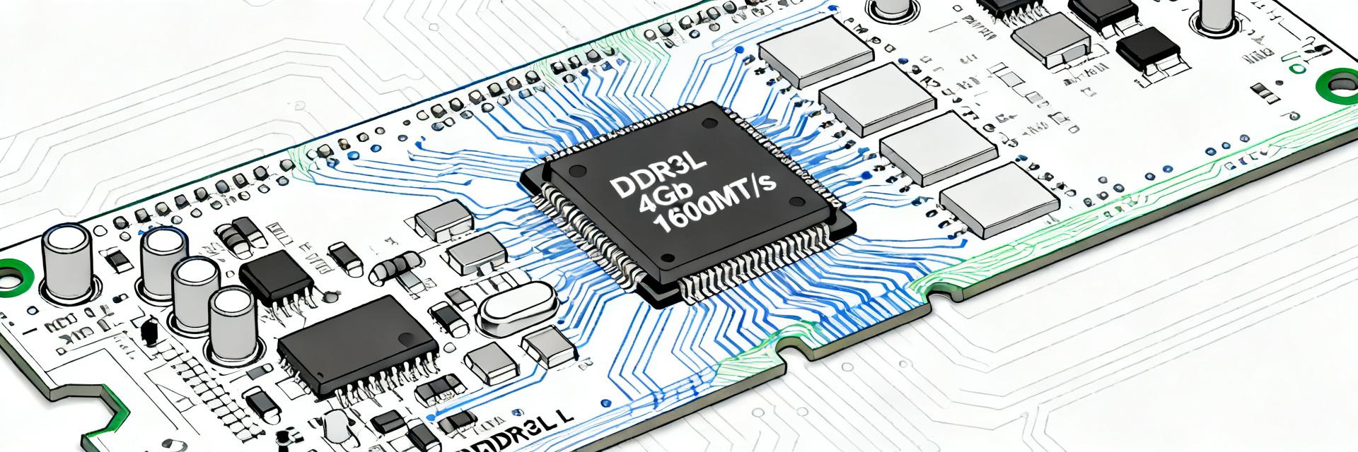
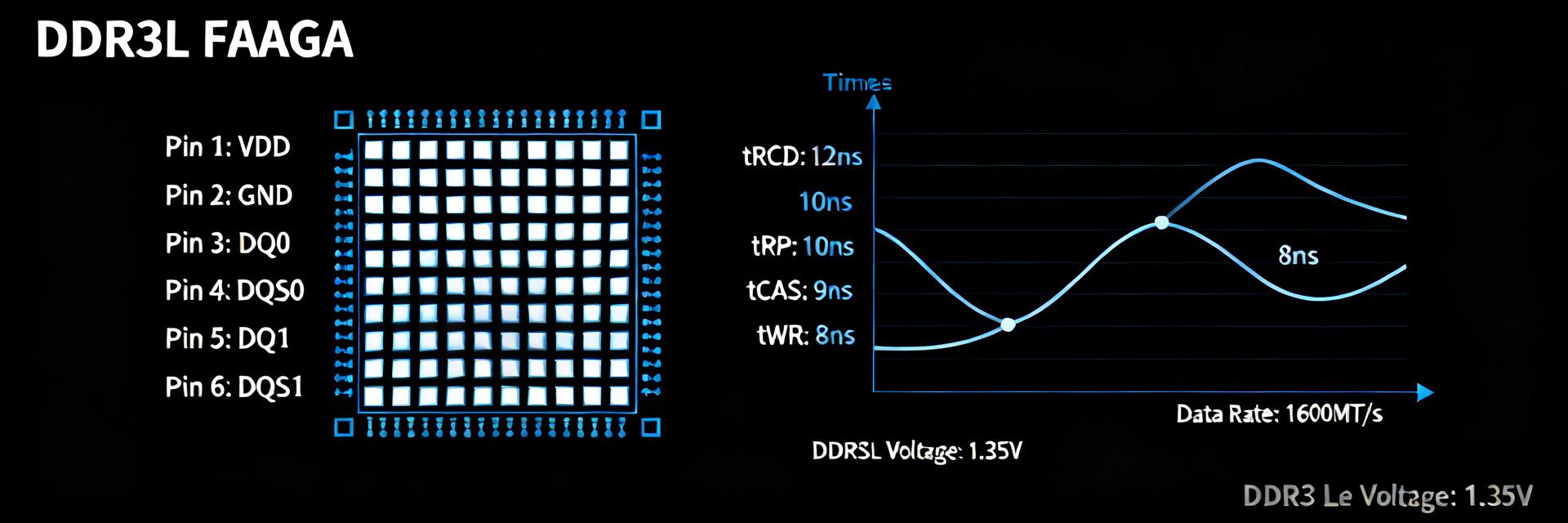
MT53D512M32D2DS-053 WT:D Datasheet Insights & Key Specs
The MT53D512M32D2DS-053 WT:D is a 16Gb LPDDR4 device organized as 512M x 32 with a rated throughput near 1866 MT/s (≈1.866 GHz clock rate) in a WFBGA package; designers evaluate it for high-bandwidth embedded memory where density, low-power modes, and compact packaging matter. This article translates datasheet tables into actionable design and sourcing guidance to shorten evaluation and reduce integration risk.
Expect a concise extraction of headline specs, the electrical and thermal envelope, timing and throughput calculations, package/pinout guidance, validation checklists, and procurement controls — all framed so an engineer can go from datasheet to lab validation efficiently.
(1 of 5) — Background & Core Specifications

What the part number encodes (organization, density, speed grade)
Point: The part string encodes organization, density and speed grade; extracting this lets engineers confirm compatibility with the memory controller. Evidence: MT53D512M32D2DS-053 decodes as 512M×32 organization → 16Gb total, and the suffix indicates the speed grade and package variant. Explanation: confirm the numeric speed-grade (the "-053" suffix) against the official datasheet so timing windows and thermal derates line up with the host controller.
| Spec | Value |
|---|---|
| Density | 16 Gb |
| Organization | 512M × 32 |
| Nominal I/O voltage | ≈1.1 V (LPDDR4 typical) |
| Data-rate | ≈1866 MT/s (nominal) |
| Package | WFBGA (ball-array) |
| Pin / ball count | Refer to datasheet ball-map (verify exact count) |
Actionable: label this table in the design folder as "MT53D512M32D2DS-053 specs" and copy datasheet figure/table references next to each value for traceability.
Electrical & thermal envelope (voltage rails, temp ranges, power modes)
Point: LPDDR4 devices list multiple rails (core and I/O), defined operating and storage temperature ranges, and low-power modes. Evidence: expected rails include VDD and VDDQ with typical nominal ~1.1 V; common features: self-refresh, deep power-down and write-leveling support. Explanation: verify the datasheet's operating and storage temperature ranges and note any extended or restricted grades — these affect board thermal design and qualification scope.
Actionable: copy the exact VDD/VDDQ ranges and all power-mode currents from the datasheet into the power budget worksheet; include a short note on how tight voltage/timing windows influence SoC PHY compatibility. Use the datasheet as the authoritative source for margining and sequencing steps.
(2 of 5) — Data Deep-Dive: Timing, Performance & Reliability
Timing parameters & throughput calculations
Point: Critical timing parameters (tCK, tRCD, tRP, tRFC, tREFI, DQS timing and CAS latency) determine achievable performance and boot training behavior. Evidence: extract the timing table from the datasheet and cross-check with the memory controller timing window. Explanation: to compute peak theoretical bandwidth use: Bandwidth (GB/s) = (MT/s × bus width in bits) / 8 / 1000 (for GB). Example: 1866 MT/s × 32 bits ÷ 8 = 7.464 GB/s peak per device.
| Timing Parameter | Notes / Action |
|---|---|
| tCK | Copy min/max values from datasheet; validate with PHY |
| CAS / CL | Record supported CAS values and training requirements |
| tRFC / tREFI | Use for refresh scheduling and controller DRAM maintenance |
Actionable: annotate the timing table with the host controller limits and flag mismatches before layout; include the datasheet table reference for each number.
Reliability, endurance & lifecycle notes
Point: Datasheet notes on JEDEC compliance, error-correction support, retention and product status inform long-term use. Evidence: LPDDR4 devices typically state JEDEC conformance and may not include on-die ECC; product status fields indicate active/legacy/obsolete. Explanation: treat "product status" as a procurement risk metric — legacy or obsolete flags require mitigation (alternate sources, redesign windows).
Actionable: log any mandatory thermal derating or mandatory cooling requirements in the BOM risk register and flag for sign-off. If MT53D512M32D2DS-053 appears as non-active in the datasheet tables, escalate to procurement immediately.
(3 of 5) — Package, Pinout & Integration Guide
Package mechanicals & pinout essentials
Point: Extract package dimensions, ball-map and mechanical tolerances for footprint verification. Evidence: datasheet mechanical drawings define package size (example dimensions often appear; always verify the exact figure). Explanation: list special pins (power rails, VREF, DQS groups) and call out pitch and critical ball groups for signal integrity checks.
Actionable: include a simplified pinout diagram in the hardware folder (referencing the datasheet figure) and attach an SVG/PNG for CAD. Verify land pattern and solder-mask openings against the datasheet's recommended footprint before layout release.
PCB layout, signal integrity & power-sequencing best practices
Point: Layout and sequencing determine training success and long-term signal integrity. Evidence: best practices include per-rail decoupling, controlled impedance traces for DQ/DQS, and length-matching DQS groups. Explanation: recommend defining plane stackup, placement of bypass capacitors, and a power-sequencing order that meets datasheet Vtt/Vref timing.
Actionable: produce a pre-layout checklist (decoupling list, plane stackup, DQS length-matching targets) and a lab validation checklist (scope probe points, training waveform capture, thermal soak test). Double-check required VREF/VTT values in the datasheet before finalizing the power-sequence timeline.
(4 of 5) — Performance Use Cases & Benchmarking
Typical application scenarios and where this part fits
Point: 16Gb LPDDR4 at ~1866 MT/s suits high-throughput embedded applications with tight area and power constraints. Evidence: density and bus width map well to multimedia SoCs, display buffers and networking buffer pools. Explanation: for streaming video or imaging, the device’s peak bandwidth and low-power modes balance throughput and energy; for low-latency tasks, consider controller PHY tuning and bank distribution.
Actionable: write short vignettes mapping expected throughput and power trade-offs for each use case and note when multiple die or wider buses are preferable.
Benchmark checklist & test-plan highlights
Point: A compact benchmark plan verifies datasheet claims and integration sanity. Evidence: tests should measure raw sustained bandwidth, random vs sequential latency, power-per-MB/s, thermal rise under load and training stability. Explanation: capture training logs and PHY calibration behaviors to judge field reliability.
Actionable: include a test-plan that logs metrics, fixture description and expected pass/fail criteria; label the document "MT53D512M32D2DS-053 performance" for traceability.
(5 of 5) — Design Validation, Compliance & Sourcing Checklist
Pre-procurement checklist & life-cycle risk controls
Point: Procurement must confirm part-identifier details to avoid mismatches. Evidence: verify full part number and suffix, revision code, temperature grade, package markings and datasheet revision. Explanation: incorrect suffix or revision can change speed grade or temperature limits and invalidate qualification.
Actionable: add mandatory line items to the purchase order: datasheet revision reference, product-status confirmation, and incoming inspection criteria (marking, lot code). Perform a board-level validation on first articles prior to design freeze.
Migration alternatives and mitigation strategies
Point: Plan for replacements and upgrades by identifying which electrical and timing fields must match. Evidence: critical match fields include nominal voltages, timing windows, I/O width and package ball-map. Explanation: some differences can be absorbed in firmware (timing regs), others require hardware changes (VTT, footprint).
Actionable: define buffer-stock targets, maintain a cross-reference table for potential replacements, and design firmware abstraction layers to reduce rework risk in the event of end-of-life notices.
Summary
Core takeaways: the MT53D512M32D2DS-053 WT:D is a 16Gb LPDDR4 device (512M×32) rated near 1866 MT/s in a WFBGA package; designers should prioritize validating the electrical envelope, timing compatibility and sourcing/lifecycle risk before committing to production.
- Electrical envelope: verify VDD/VDDQ ranges and power-sequence timing from the datasheet into the power budget and BOM risk register.
- Timing compatibility: extract tCK, CAS, tRFC and DQS timing and compare directly to the SoC PHY; perform the throughput calc and training tests in the lab.
- Sourcing & lifecycle: confirm full part suffix/revision, datasheet revision, and product status; plan buffer stock and alternate cross-references.
Frequently Asked Questions
What is the peak bandwidth of MT53D512M32D2DS-053 WT:D?
Peak theoretical bandwidth = data-rate × bus width / 8. For 1866 MT/s on a 32-bit bus that equals about 7.464 GB/s. Real sustained bandwidth will be lower; use the benchmark checklist to quantify usable bandwidth under your access pattern.
What package and footprint does MT53D512M32D2DS-053 WT:D use?
The device is supplied in a WFBGA ball-array package; confirm exact dimensions and ball-map from the datasheet mechanical drawings before PCB layout. Create the footprint per the recommended land-pattern and include solder-mask and paste stencil notes in the CAD files.
How to validate timing compatibility with a host controller for MT53D512M32D2DS-053 WT:D?
Extract critical timing fields (tCK, tRCD, tRP, tRFC, DQS timing) from the datasheet and compare to the controller's supported windows. Run PHY training, capture DQS eye and latency under representative traffic, and record pass/fail against documented thresholds in the test-plan.
What are the primary power supply rails required for this LPDDR4?
LPDDR4 typical operation utilizes core rails including VDD1 (typically 1.8V nominal), VDD2 (typically 1.1V nominal), and the I/O rail VDDQ (typically 0.6V nominal). Voltage stability is critical for signal integrity and PHY calibration.