MT41K512M8RH-125 DDR3L Datasheet: Key Specs & Stats
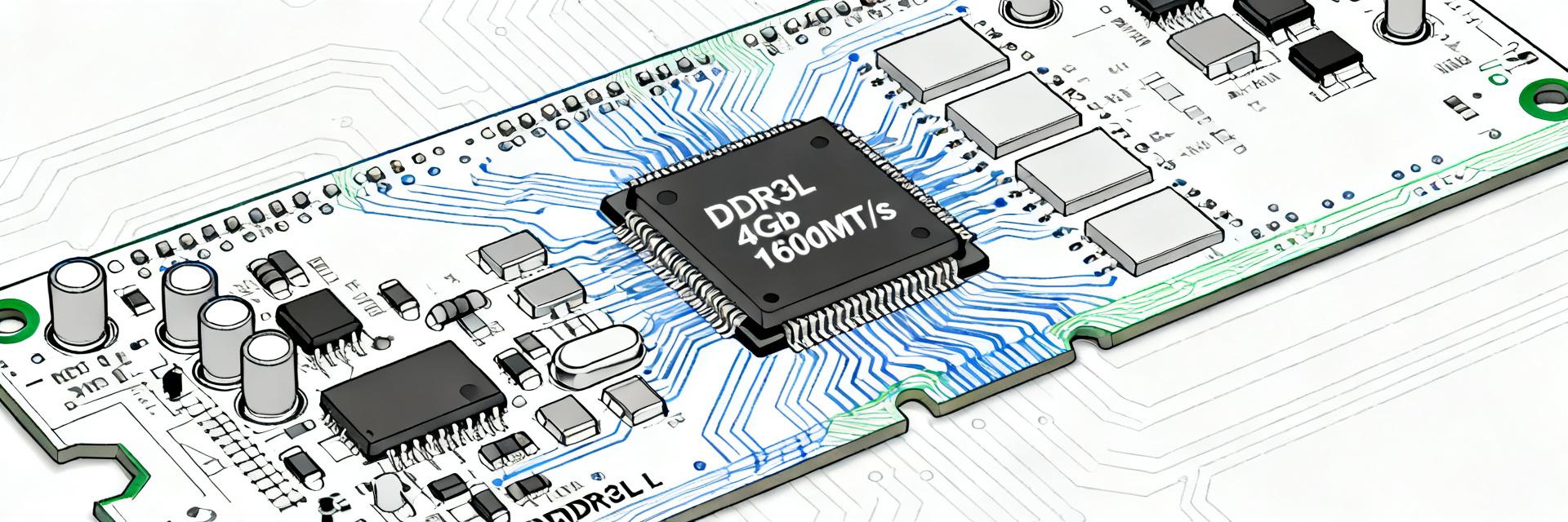
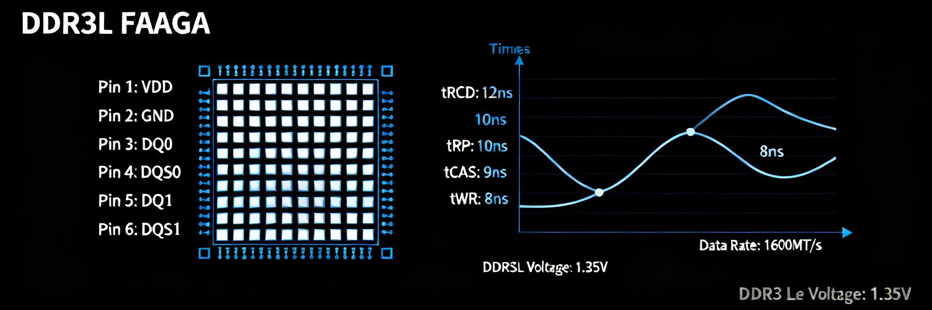
The MT41K512M8RH-125 delivers a 4Gb device organized as 512M x 8, targeting DDR3-1600 class systems with an I/O clock at 800 MHz and typical access latency near 13.75 ns. It operates at a nominal 1.35V DDR3L voltage, offering a clear voltage and density profile for low-power embedded designs. This datasheet-focused review explains why those headline numbers matter for system architects: power savings relative to standard DDR3, high bit density for constrained board area, and a practical performance envelope for mid-range SoC memory subsystems. Readers will get a concise breakdown of electrical and timing parameters, organization and packaging guidance, PCB integration best practices, a real-world integration scenario, and a compact validation checklist — all framed to support design decisions and verification planning.
Key terms used here include the part number and DDR3L class; engineers should treat this as a guided reading of the official datasheet tables and figures for exact test-condition numbers and qualification notes. The article emphasizes which datasheet tables to consult for currents, timing, and mechanical land pattern data and provides actionable recommendations for integration and test.
1 — Product overview & quick spec summary (background)
1.1 — One-line part summary
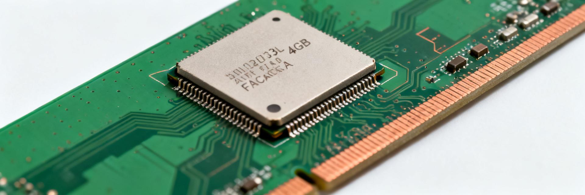
MT41K512M8RH-125 is a 4Gb DDR3L SDRAM organized as 512M x 8 and supplied in an FBGA package class appropriate for high-density BGA mounting. It’s rated for 1.35V operation and an 800 MHz I/O clock (DDR3-1600 class); consult the datasheet mechanical table for exact ball count and footprint class. Action: verify package variant marking against your board footprint early in the BOM review.
1.2 — Typical use cases & compatibility notes
This density and voltage class suits mobile modules, embedded controllers, and network-attached SoCs where board area and power matter. DDR3L signals remain electrically compatible with many DDR3 memory controllers with proper voltage/ODS handling; however, confirm controller Vdd/Vddq support and ODT options. Action: map your controller’s supported timing table to the device speed grade before layout.
2 — Key electrical & timing specifications at a glance (data analysis)
| Parameter / Feature | Datasheet Value (MT41K512M8RH-125) |
|---|---|
| Density & Configuration | 4Gb (512 Meg x 8) |
| Nominal Supply Voltage (VDD/VDDQ) | 1.35V (DDR3L) - Backward compatible with 1.5V |
| I/O Clock / Speed Grade | 800 MHz / -125 (DDR3-1600 Class) |
| Internal Banks | 8 banks |
| Standard Latency Envelope | CL-11-11-11 (tAA = 13.75 ns) |
| Packaging Option | 78-ball FBGA (RH variant) |
2.1 — Core electrical specs
The part’s nominal Vdd/Vddq is 1.35V with defined operating ranges and standby/self-refresh states documented in the datasheet’s electrical characteristics. The datasheet lists currents for active, precharge, and self-refresh modes under specified I/O conditions; use those numbers to size PMIC and decoupling budgets. Action: allocate PDN margin for worst-case active current plus routing loss, and follow the datasheet’s supply-sequencing notes during bring-up.
2.2 — Speed grades & timing (latency)
Rated for an 800 MHz I/O clock (DDR3-1600), timing parameters such as tCK, tRCD, tRP and tRAS are provided in timing tables; the datasheet’s typical access time is ~13.75 ns, which maps to system latency expectations at common CAS settings. Impact: tighter CAS and tRCD values reduce latency but tighten timing margins — action: plan for controller calibration and margin analysis using the datasheet timing examples.
3 — Memory organization, addressing & packaging details (data analysis)
3.1 — Logical organization & addressing
The device organizes memory into multiple banks with row/column addressing consistent with standard DDR3 command sets; data width is x8, so a single device provides eight-bit-wide data lanes. The datasheet specifies burst length, bank count and address mapping tables; check those to size interleaving and rank strategies. Action: align controller address mapping to the device’s bank and row/column scheme to avoid addressing errors.
3.2 — Package & mechanical footprint
Packaged in FBGA/BGA, the datasheet includes a mechanical drawing with ball count, pitch, and recommended land pattern; thermal pad and placement notes highlight solder reflow and thermal conduction considerations. Action: match your PCB land pattern and solder mask to the exact datasheet footprint and verify reflow profile against the package thermal limits.
4 — Thermal, reliability & operating conditions (method guide)
4.1 — Operating & storage temperature ranges
The datasheet lists commercial and, where available, industrial temperature ranges and corresponding derating guidance. Operating temperature affects refresh rate and retention margin; plan thermal management to keep junction temperature within the specified operating window. Action: simulate worst-case power dissipation and validate board airflow or heatsinking strategies against the datasheet thermal guidance.
4.2 — Reliability metrics & lifecycle considerations
Refresh requirements and expected retention behavior are covered in the datasheet; designers should consult the reliability and qualification sections for JEDEC-aligned test flows and any MTBF/qualification notes. Action: include refresh verification and retention stress tests in your qualification plan, and record which datasheet sections govern production test limits.
5 — PCB integration & layout best practices (method guide)
5.1 — Power delivery & decoupling recommendations
Follow the datasheet decoupling table for recommended capacitor values and placement: bulk caps on the board edge and high-frequency decouplers close to the package Vdd/Vddq pins. Supply sequencing notes in the datasheet should be implemented by the PMIC. Action: place 0.1µF and higher-frequency caps within millimeters of power pins and verify PDN impedance targets in simulation or lab measurement.
5.2 — Signal routing & termination tips
Length-matching for address/command lines and controlled impedance for DQ/DQS are essential; the datasheet suggests ODT settings and termination strategies to reduce reflections. Action: match DQS/DQ groups tightly, use differential routing where required for strobe pairs, and validate signal integrity with IBIS/behavioral models referenced in the datasheet.
6 — Real-world integration example (case display)
6.1 — Example: embedded module memory subsystem
Selecting this 4Gb DDR3L part for a mid-performance embedded board balanced density and power: 1.35V operation reduced PDN stress compared to DDR3, while 800 MHz I/O met throughput targets. Key checks included verifying footprint, thermal headroom, and controller timing tables from the datasheet. Action: document these verification checkpoints in the design review.
6.2 — Verification steps performed
Bench tests included power-up sequencing verification, write/read margin sweeps, timing calibration runs, and temperature cycling to catch early failures. Each test referenced the datasheet’s electrical and timing tables for pass/fail criteria. Action: capture margin plots and failure logs for regression testing and production sign-off.
7 — Datasheet reading checklist & engineering action plan (action advice)
7.1 — Quick datasheet checklist (engineer’s 8-point list)
Confirm part/package variant, voltage ranges and PDN requirements, timing tables required by the memory controller, thermal derating data, footprint match, ODT/termination settings, recommended test patterns, and production qualification notes. Action: map each item to the specific datasheet table or figure during design review and sign off.
7.2 — Common pitfalls & troubleshooting tips
Typical fixes include tightening decoupling near power pins when marginal currents appear, reworking address/command length mismatches, and recalibrating ODT/CAS settings for intermittent errors. Action: when encountering instability, reproduce at elevated temperature and log eye/margin metrics against datasheet timing windows.
Summary
In summary, MT41K512M8RH-125 is a 4Gb (512M x 8) DDR3L device optimized for lower-voltage systems, rated at an 800 MHz I/O class with a typical access time around 13.75 ns. That combination yields meaningful power savings versus legacy DDR3 while delivering high density for area-constrained boards. The datasheet should be your single source for electrical characteristics, timing tables, mechanical footprint, and reliability notes; follow its PDN, decoupling, and routing recommendations and validate with the outlined bench tests to ensure robust integration.
- Device profile: 4Gb, x8 organization and 1.35V DDR3L operation — confirm package variant and footprint against the datasheet prior to layout.
- Electrical/timing priorities: consult timing tables for tCK/tRCD/tRP and use the ~13.75 ns access-time figure to set system latency targets and controller calibration.
- Integration checklist: implement datasheet decoupling and supply sequencing, match trace lengths for DQ/DQS, and run power-up, margin, and thermal stress tests before production.
Frequently Asked Questions
What is the organization and operating voltage of the MT41K512M8RH-125?
The MT41K512M8RH-125 is organized as a 512M x 8 device (4Gb density) operating at a nominal low voltage (DDR3L) of 1.35V, while remaining backward compatible with standard 1.5V environments.
How does DDR3L voltage save power compared to standard DDR3?
By operating at 1.35V instead of 1.5V, DDR3L reduces thermal overhead and dynamic power dissipation significantly, allowing longer battery life and simplified heat dissipation for embedded modules.
What are the key timing parameters for the DDR3-1600 speed grade?
The -125 speed grade runs at an 800 MHz clock speed, mapping to DDR3-1600 class performance. Typical access latency (tAA) is 13.75 ns under JEDEC standard CAS settings (CL-11).
What routing guidelines apply to DQ and DQS signals?
Keep byte lanes grouped together, match routing lengths within standard tolerance bounds, use differential routing for strobe lines (DQS/DQS#), and optimize signal termination (ODT) values to prevent reflections.