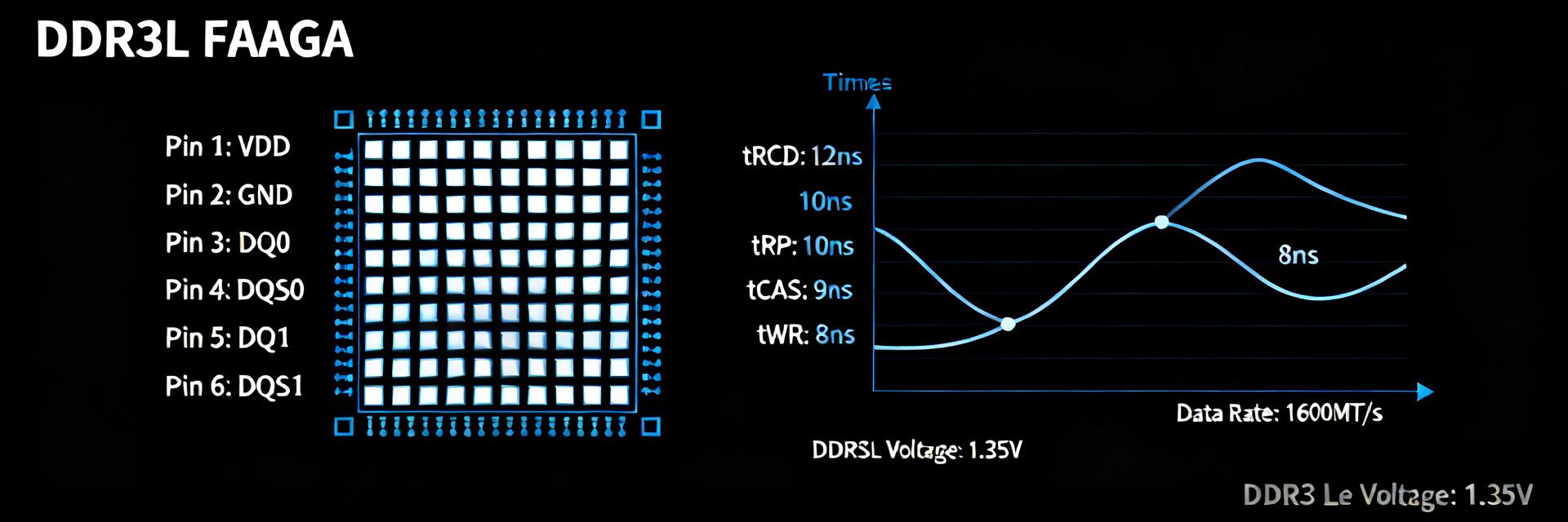
MT53E768M32D4DT-053 Datasheet: Complete Specs & Pinout
The MT53E768M32D4DT-053 is a 24 Gbit (768M x 32) LPDDR4 mobile memory device rated for high-bandwidth, space-constrained applications. Its top data-rate capability and compact 200-ball FBGA package make it suitable for handheld and embedded designs where power envelope, thermal dissipation, and routing density are critical. This page condenses the official datasheet and a practical pinout guide.
This article provides a single-page walkthrough of the datasheet, an interpreted pinout, an integration checklist for PCB layout and SI, and verification tips for engineers. Expect concise tables, an annotated pin grouping summary, layout checklists, and a short validation plan tailored for system integration and risk reduction.
1 — Product snapshot & core specs
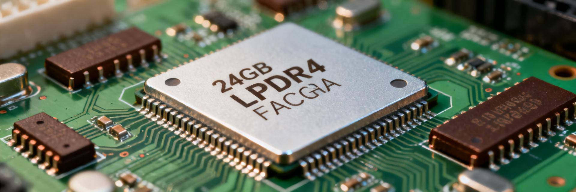
Key electrical and functional specs
Key specs at a glance: density 24 Gbit organized as 768M x 32; LPDDR4 architecture; peak DDR interface clock up to ~1866 MHz (effective data rate dependent on timing grade); supply rails centered on 1.1 V (VDD/VDDQ typical); 200-ball FBGA package; commercial and extended temperature grades noted in the datasheet. Designers should plan for nominal active currents and standby currents with margin when budgeting power.
| Attribute | Value / Note |
|---|---|
| Organization | 768M x 32 (24 Gbit) |
| Memory Type | LPDDR4 |
| Effective Data Rate | Up to ~1866 MHz (device/grade dependent) |
| Voltage | VDD / VDDQ ≈ 1.1 V (refer to datasheet) |
| Package | 200-ball FBGA |
| Typical Use | Mobile, embedded, space-constrained high-bandwidth systems |
Typical applications & form-factor considerations
This device suits smartphones, tablets, compact vision modules, and embedded compute where LPDDR4’s low voltage and high throughput are needed. The FBGA footprint reduces board area but increases thermal and reflow constraints; ensure proper thermal vias and solder-mask clearances. Low-power modes and burst characteristics make it preferable where aggressive power management is required.
2 — Electrical characteristics & timing
Power rails, current, and thermal limits
VDD and VDDQ nominally target ~1.1 V; absolute ranges and max ratings are defined in the datasheet and must be respected. Typical active and standby currents vary by speed grade—designers should budget for peak write/read current surges plus decoupling headroom. Maintain ambient and junction thermal margins; FBGA thermal path requires plated vias under the die area where specified.
Timing parameters and performance (CL, tCK, burst, frequency)
Critical timing includes clock period (tCK), CAS-latency equivalents, and burst length behavior. For example, at a 933 MHz clock (1.866 Gbps effective), effective bandwidth per 32-bit device ≈ (1.866 Gbps × 32) / 8 = ~7.464 GB/s theoretical peak. Real achievable throughput is lower due to command overhead, refresh, and controller efficiency—use timing tables to map speed grade to usable bandwidth.
3 — Pinout & package map
Annotated pinout diagram: power, address, data, control pins
The MT53E768M32D4DT-053 pinout groups power/ground, command/address, data lanes, and reference pins across the FBGA. Power balls (VDD/VDDQ) are distributed to minimize IR drop; GND is abundant. Command/address pins (CS_n, RAS_n, CAS_n equivalents for LPDDR4 command mapping) and CA lanes should be routed with attention to skew. Reset and mode pins must be tied per datasheet sequencing requirements.
| Pin Group | Function / Notes |
|---|---|
| VDD / VDDQ | Primary supplies; place local decoupling |
| GND | Return plane; short loops |
| CA / CMD | Command/address routing; length-matched where required |
| DQ / DQS | Data lanes and strobes; strict timing and routing |
| REF / TERM | On-die termination reference pins; follow placement guidance |
PCB footprint and mechanical notes
FBGA ball pitch and solder pad dimensions require controlled solder paste volume and mask openings. Recommend thermal via array under the exposed pad area if present; maintain solder-mask expansion per vendor recommendations. Common mistakes: insufficient via stiching, incorrect stencil aperture for center balls, and lack of board warpage control during reflow—use manufacturer footprint notes as the authoritative source.
4 — System integration & layout best practices
Power sequencing, decoupling, and rails
LPDDR4 parts require defined power-up and power-down sequences; order and timing of VDD/VDDQ and I/O rails affect device reliability. Place multiple decoupling capacitors close to each power ball: bulk capacitance a few millimeters away, high-frequency ceramic 0201/0402 caps within 1–2 mm of pads. Include power-good monitors and test points for VDD, VDDQ, and VTT (if applicable).
Signal integrity: routing, termination, and clocking tips
Match trace lengths across data strobes and related DQ lines; ensure differential pairs (if applicable) maintain consistent impedance. Place termination resistors near the device where the datasheet recommends and avoid stubs on high-speed nets. Validate with simulation: eye diagrams, channel loss, and crosstalk checks should be part of pre-layout and post-layout verification.
5 — Validation, testing & lifecycle considerations
How to validate a board against the datasheet
A practical test plan starts with power sequencing verification and passive checks (voltages, continuity). Proceed to controller initialization, then functional memory training at the intended speed grade. Use a logic analyzer, DDR memory controller testbench, and thermal soak to confirm behavior under load. Compare measured currents and timing margins against datasheet tables and log any deviations for corrective layout or firmware changes.
Obsolescence, sourcing notes & replacement strategy
Confirm lifecycle and obsolescence status via the manufacturer's official part detail page and maintain a cross-reference table in project documentation. If the part becomes unavailable, identify drop-in replacements by matching density, organization, timing grade, voltage, and package. Document rationale for any equivalent part choice and update BOM control files accordingly.
Summary
- The MT53E768M32D4DT-053 summary consolidates the device’s LPDDR4 24 Gb organization, 200-ball FBGA footprint, and power/timing constraints to accelerate design reviews and layout decisions.
- Use the datasheet’s timing and current tables to size decoupling, set sequencing, and validate thermal strategies early in the design cycle.
- Follow the provided pin grouping and layout checklist—power placement, short return paths, thermal vias, and matched DQ/DQS routing—to reduce integration risk.
Frequently Asked Questions
What are the critical power rails and sequencing notes from the MT53E768M32D4DT-053 datasheet?
Critical rails include VDD and VDDQ at ~1.1 V; strict sequencing is required to avoid latch-up and to ensure proper device initialization. Designers should verify the datasheet-specified order and delays, place local high-frequency decoupling near power balls, and provide power-good monitoring points. Always test sequencing on a bench before full system bring-up.
How should an engineer verify timing and throughput for this LPDDR4 part?
Validate timing by running memory controller training at the target speed grade, measure read/write latencies, and capture eye diagrams with an oscilloscope or serial-link tester. Calculate theoretical bandwidth from effective data rate and bus width, then measure sustained throughput under realistic traffic patterns to account for refresh and command overhead.
What layout pitfalls commonly cause failures with FBGA LPDDR4 devices?
Common failures arise from poor decoupling placement, insufficient thermal vias, mismatched data lane lengths, and inadequate termination placement. Avoid long stubs, keep CA and DQ groups length-matched as specified, and ensure the stencil and solder paste apertures are tuned to prevent tombstoning or voiding on interior balls.
What is the peak theoretical bandwidth of the MT53E768M32D4DT-053 LPDDR4?
The theoretical peak bandwidth is approximately 7.464 GB/s per 32-bit device. This is derived from an effective clock frequency of 1.866 Gbps running over a 32-bit wide memory interface, computed via the standard formula: (1.866 Gbps * 32) / 8.