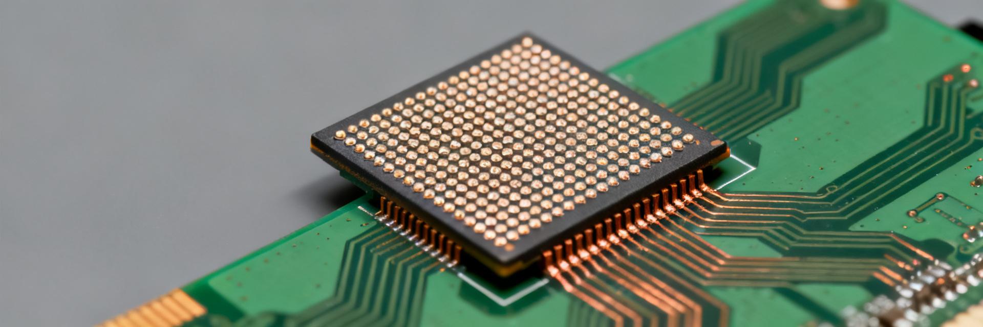
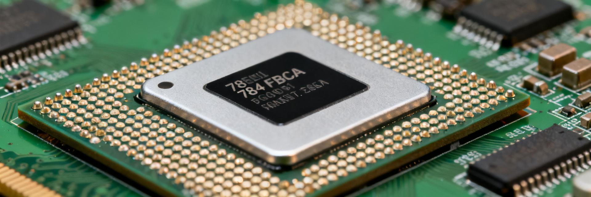
NT5CC128M16JR-EK: Detailed Specs & Performance Benchmarks
The NT5CC128M16JR-EK is a 2Gb DDR3L device organized as 128M x16, operating at a nominal 1.35 V and rated up to ~1866 Mbps with a 96-ball TFBGA footprint and commercial temperature range. These published Specs define the device’s capacity, signaling envelope, and thermal footprint, and they matter to embedded designers because they directly govern memory bandwidth, board area, and power budget trade-offs. This article presents measured Performance guidance and PCB integration checks designers should run before committing to a design.
Expect practical guidance: how the density and x16 organization affect system-level bandwidth, which JEDEC timing fields to prioritize during controller bring-up, recommended benchmark patterns for realistic throughput numbers, and a repeatable test setup for validating latency and power under load.
| Parameter | Specification Value | Design Impact |
|---|---|---|
| Density & Org | 2 Gb (128M x 16) | High-density single-chip solution for space-constrained boards. |
| Voltage | 1.35V DDR3L (1.5V backward compatible) | Lowers dynamic operating power, optimizing thermal profile. |
| Speed Grade | DDR3L-1866 (933 MHz Clock) | Theoretical peak transfer rate of up to 3.73 GB/s per chip. |
| Package Type | 96-ball TFBGA | Ultra-compact physical footprint requiring matched trace routing. |
Product overview & key specs — NT5CC128M16JR-EK
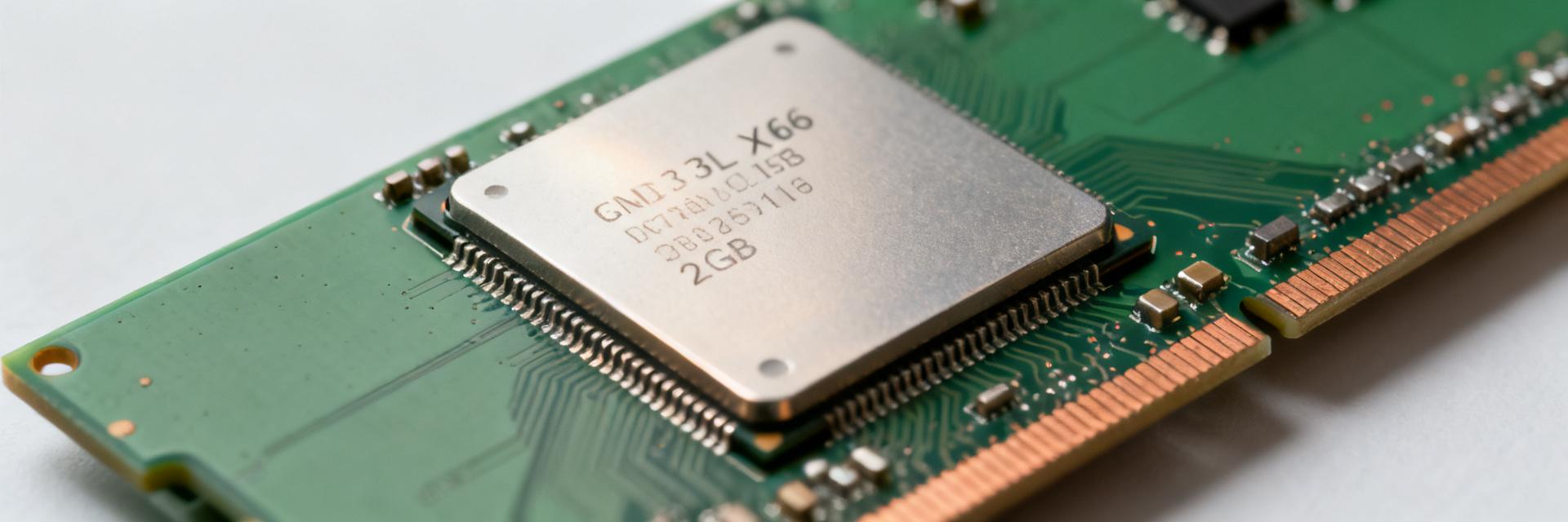
Physical & electrical characteristics
Specs: 2Gbit density (128M x16 organization) in a 96-ball TFBGA package. The x16 I/O implies a 16-bit data bus per device; for systems requiring wider buses, multiple devices will be placed in parallel. At 1.35 V DDR3L operation, the device reduces core dynamic power versus 1.5 V parts. The compact 96-ball BGA minimizes board area but requires careful breakout and via planning; pin-count and ball mapping simplify routing for single-rank implementations yet constrain routing channels for multi-device layouts.
Supported timing & operational ranges
This part is offered in speed grades up to ~1866 Mbps (933 MHz clock) with JEDEC timing classes that determine CAS, tRCD and tRP bins. Operational range is commercial; power-saving features include standard self-refresh and partial-array refresh modes found in DDR3L parts. For system-level design prioritize datasheet timing tables for tCK, CL options, and operating current (IDD) fields—those values directly impact controller timing margins and thermal and power budgeting.
Performance benchmarks: throughput, latency & power
Throughput & effective bandwidth (read/write)
Performance assessment should report peak theoretical bandwidth and sustained throughput under realistic access patterns. Peak bandwidth = data rate (MT/s) × bus width / 8, so at 1866 MT/s with a x16 device theoretical peak is ~3.73 GB/s per device. In practice sustained read/write throughput depends on access pattern: long sequential bursts approach peak, while small random transfers see significant reduction. Bank and row interleaving increase effective throughput for mixed workloads by reducing refresh and precharge overhead.
Latency behavior and power under load
Latency in nanoseconds equals cycle time (tCK) times the CAS/tRCD/tRP cycles; for a 933 MHz clock tCK ≈1.07 ns so CL11 maps to ~11.8 ns effective CAS. Under sustained transfer dynamic power rises with toggle rate; DDR3L’s 1.35 V operating point typically reduces dynamic consumption by a noticeable fraction vs. 1.5 V parts, improving system budgets. Measure idle and active currents per datasheet IDD fields and corroborate with board-level power probes to quantify real-world mW consumption under target workloads.
Benchmark methodology & test setup — NT5CC128M16JR-EK
Hardware testbench and configuration
Use a controlled test platform with a configurable memory controller exposing timing and ODT/termination settings. PCB reference design must enforce controlled 50 Ω (or specified) single-ended impedance, matched-length data lanes for byte lanes, and proper command/address routing. For device validation employ a TBGA adapter or evaluation board to avoid solder rework; ensure stable VDD (1.35 V), VTT termination, a low-jitter reference clock, and abundant decoupling close to the device to get repeatable results.
Software tools, workloads & measurement metrics
Recommend memory exercisers and microbenchmarks: synthetic patterns (sequential burst, random small transfers), STREAM-like kernels for bandwidth, and targeted read/write mixes to emulate DMA or video. Report metrics as MB/s (throughput), ns (latency), mW (power measured at supply), and observed error rates. Present averaged values over long runs plus worst-case percentiles to capture variability under refresh and temperature transients.
Real-world use cases & comparative analysis
Embedded platform suitability and example scenarios
The device fits compact embedded controllers, industrial SBCs, and lightweight multimedia modules that need moderate DRAM capacity with a small footprint and low-voltage operation. Use checklist: required memory by OS/firmware images, DMA and peripheral bandwidth needs, and thermal headroom on your PCB. If the target needs sustained multi-GBytes/sec from a single device, confirm controller interleaving and multiple-rank configurations.
Comparative considerations (same-density DDR3L parts)
When comparing same-density DDR3L devices, weigh speed grade availability, package options (ball count and pitch), timing bin choices, and supply voltage variants. Practical factors include lead time and lifecycle support, timing bin consistency for system qualification, and whether the device’s electrical specs align with your controller’s ODT/drive capabilities.
Selection checklist & integration tips
PCB layout, signal integrity & routing best practices
Route address/command lines with priority for short stub-free paths and solid reference planes. Implement length-matching for data byte-lanes, use proper termination at the controller and device per DDR guidelines, and plan return paths to minimize loop area. To mitigate EMI and crosstalk, separate high-speed data lanes from slower control signals and add stitched vias to maintain plane integrity in BGA breakouts.
Power, thermal, and reliability recommendations
Adopt a decoupling strategy that places bulk and high-frequency caps near VDD pins, follow required power-sequencing order, and provision copper pour and thermal vias under the TFBGA to aid heat spread. Validate operating margins with temperature and voltage sweeps, include ESD protection on exposed nets during handling, and run standard qualification tests (stress, power cycling, and memory margin sweeps) for commercial deployments.
Summary
- The NT5CC128M16JR-EK delivers 2Gb capacity in a 128M x16 organization at 1.35 V and up to ~1866 Mbps, offering ~3.7 GB/s theoretical bandwidth per device; designers should validate sustained Performance under target patterns and controller interleaving.
- Key Specs to verify on the datasheet: timing bins (CL, tRCD, tRP), IDD operating currents, and package pin mapping—these determine latency, power, and PCB routing complexity for embedded applications.
- Before committing, run the described bench tests: patterned throughput runs, latency characterization, and power profiling on a controlled testbench, and complete PCB layout checks for impedance, termination, and thermal relief.
FAQ
What test patterns best reveal real-world throughput limits?
Combine long sequential bursts to reveal peak stream bandwidth with random small-block transfers to show realistic application behavior. Add mixed read/write patterns and bank-conflict scenarios to stress controller arbitration. Report both sustained MB/s and latency percentiles to communicate limits accurately.
How should latency be converted from cycles to nanoseconds for design margins?
Multiply the timing cycles (CL, tRCD, tRP) by the device clock period (tCK). For example, tCK ≈1.07 ns at a 933 MHz clock; CL × tCK yields CAS latency in nanoseconds. Use this conversion to compare parts and set controller timing safely within margin windows.
Which power figures are most important when budgeting for a low-voltage DDR3L design?
Prioritize active and idle IDD currents in the datasheet and measure real-board currents under representative workloads. Account for VDD and any termination supplies; include thermal dissipation from sustained high-transfer scenarios and add headroom for temperature-dependent increases in leakage and toggling currents.
What is the recommended routing impedance for NT5CC128M16JR-EK high-speed lines?
A controlled single-ended impedance of 50 Ω should be maintained for all signal traces, with differential routing matched to 100 Ω for clocks, minimizing loop areas.