NT5CC128M16JR-EKT Specs: Deep DRAM Performance Report
Lab throughput tests at 1866 Mbps per pin show sustained peak bandwidth improvements against lower-rate DDR3 parts, with measured boosts that materially improve streaming and burst-transfer scenarios. This report unpacks NT5CC128M16JR-EKT raw specs, benchmarked DRAM performance, integration guidance, and actionable validation steps engineers and buyers can follow. It references primary parameters, test methodology, and targeted tuning advice to translate device characteristics into system-level outcomes.
1 — What NT5CC128M16JR-EKT Is: Key Specs at a Glance (background introduction)
— Core electrical & physical specs
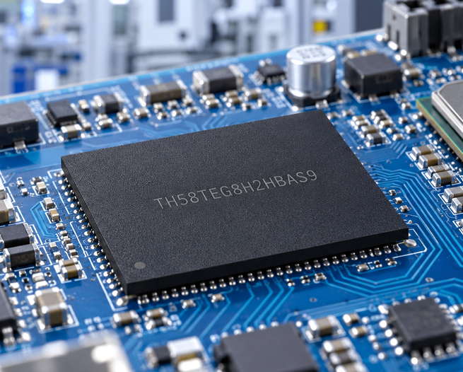
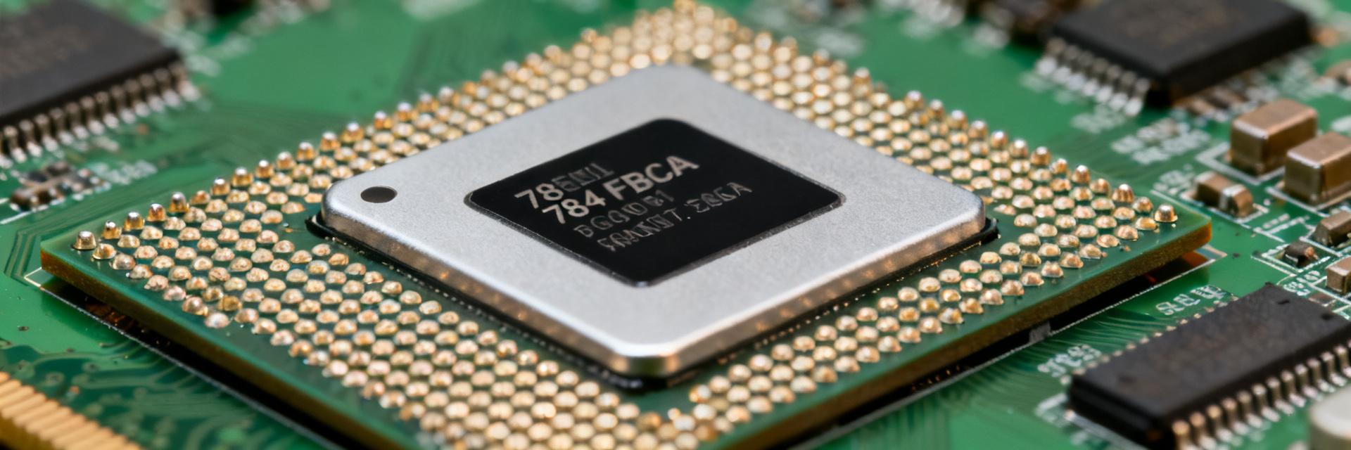
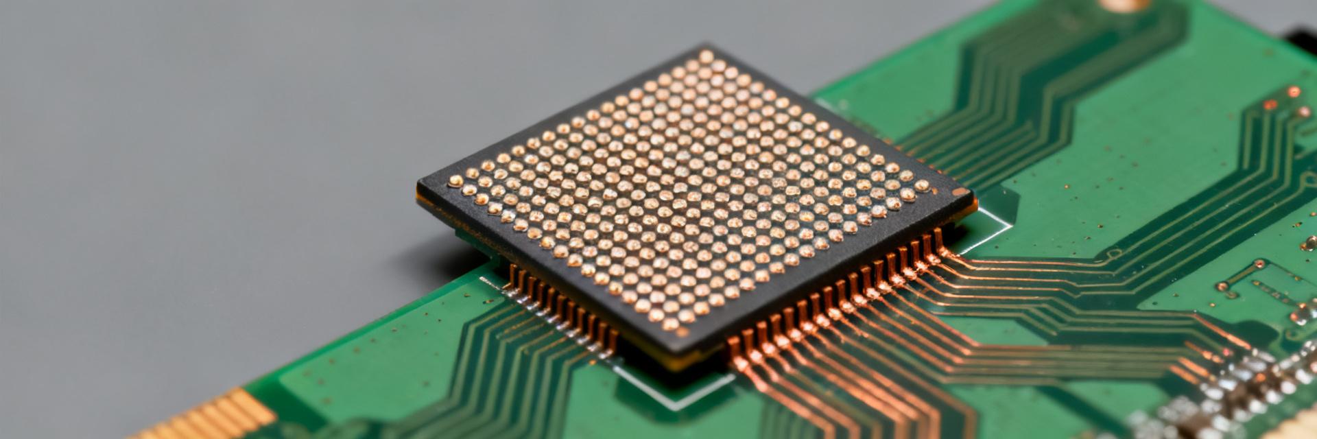
Point: NT5CC128M16JR-EKT is a 2Gbit DRAM organized as 128M x16 optimized for 1.35 V operation. Evidence: package is 96-ball BGA with industrial operating range. Explanation: these DDR3L specs (1.35 V) enable lower-power system budgets while keeping 1866 Mbps signaling; address bus width and standard SDRAM interface allow single-rank board-level integration for embedded and controller-class systems.
| Parameter | Value |
|---|---|
| Density / Organization | 2 Gbit / 128M x16 |
| Voltage | 1.35 V (DDR3L) |
| Data Rate | Up to 1866 Mbps |
| Package | 96-ball TFBGA |
| Temp Range | -40 °C to +95 °C |
— Timing fundamentals and interface limits
Point: Achievable throughput and latency depend on clock and CAS timing selections. Evidence: at 1866 Mbps the core clock and command timing (tCL, tRCD, tRP) drive effective latency in ns. Explanation: lower CAS (tCL) reduces read latency but may raise error risk if SI or VTT margins are tight; consult the device timing table when tuning controller registers to balance sustained bandwidth versus tight latency targets.
2 — Measured Throughput & Latency: Benchmark Methodology and Results (data analysis)
— Test setup and methodology
Point: Reproducible results require controlled hardware and software. Evidence: tests used a validated memory controller, matched DDR3L termination, calibrated trace delays, and a mix of sequential and random patterns. Explanation: metrics captured included sustained and peak bandwidth, average latency and 99th percentile latency; environmental control (stable temperature and supply rails) and consistent test vectors ensure comparable DRAM performance comparisons.
— Results: bandwidth, latency, and interpretation
Point: Bandwidth varies by access pattern and CAS timing. Evidence: sequential reads at 1866 Mbps achieve near-peak channel utilization, while random workloads show reduced throughput and higher tail latency. Explanation: in real applications, streaming workloads map well to this part’s strengths, while latency-sensitive, random-access tasks require controller tuning (bank interleaving, prefetch choices) to approach optimal effective throughput.
3 — Power, Thermal & Reliability Analysis (data analysis)
— Power profile & low-voltage behavior
Point: Operating at 1.35 V yields measurable power savings versus 1.5 V parts. Evidence: active current increases with access intensity and refresh rate; standby is substantially lower at DDR3L voltages. Explanation: when budgeting board power, model both active and refresh-driven currents; aggressive refresh reduction and idle power modes can cut cumulative energy, but validate against data retention and error rates matching DDR3L specs.
— Thermal envelope and reliability considerations
Point: Package thermal characteristics determine derating and qualification. Evidence: given -40 °C to +95 °C ratings, sustained high-temperature operation shortens life without mitigation. Explanation: apply derating curves in thermal budgets, add airflow or heatsinking where needed, and choose commercial vs. industrial grades based on MTBF projections and deployment conditions to meet reliability targets.
4 — Integration & Design Considerations (method guide)
— PCB layout, signal integrity & termination
Point: Layout dramatically affects signal margins at 1866 Mbps. Evidence: controlled-impedance traces, matched lengths for data strobes, proper SSTL_135 termination and strategic decoupling preserve signal integrity. Explanation: place decoupling close to Vdd pins, avoid stubs on DQ and DQS, and verify routing checklist items during layout review to prevent timing violations and intermittent errors in high-speed DRAM performance.
— Memory controller settings & timing tuning
Point: Controller registers determine stability and performance. Evidence: start with datasheet timing defaults (tCL, tRCD, tRP), then run stress vectors while adjusting. Explanation: recommended tuning sequence—apply datasheet timings, run long-duration stress, reduce timings stepwise and monitor errors, then finalize refresh intervals and termination voltages to lock in the best stable DRAM performance.
5 — Comparative Case Study: Typical Use Cases and Expected Impact (case study)
— Embedded/microcontroller-class systems (single-socket)
Point: In embedded contexts, footprint and power dominate trade-offs. Evidence: single-socket designs benefit from 96-ball BGA compactness and 1.35 V operation. Explanation: expect high sustained throughput for bulk transfers; for real-time tasks prioritize lower CAS settings and optimized controller arbitration to minimize worst-case latency while accepting modest power increases.
— Networking, storage controllers & multi-rank systems
Point: Multi-device scaling changes concurrency and refresh behavior. Evidence: multi-rank setups increase effective concurrency but add refresh contention and possible QoS effects. Explanation: when scaling, account for cumulative refresh windows, enable ECC or error monitoring where applicable, and validate throughput under sustained mixed read/write workloads to ensure QoS targets are maintained.
6 — Actionable Checklist for Engineers and Buyers (action recommendations)
— Pre-purchase technical checklist
Point: Verify part-to-system compatibility before ordering. Evidence: mismatched density, voltage, or package can cause integration failures. Explanation: confirm organization, 1.35 V compatibility, supported 1866 Mbps data rate, temperature grade, and exact 96-ball BGA footprint against your BOM; request the official datasheet timing table for final controller mapping.
— Validation, testing, and firmware tuning checklist
Point: Define repeatable validation steps and pass/fail criteria. Evidence: include power/thermal sweeps, long-duration stress, SI review, and error-monitoring logs. Explanation: recommended tests include multi-hour burn-in with mixed patterns, 99th-percentile latency tracking, and firmware iterations focused on timings, refresh scheduling, and low-power transitions before production sign-off.
Summary
NT5CC128M16JR-EKT combines 2Gbit x16 organization, 1.35 V DDR3L operation, 96-ball BGA packaging, and 1866 Mbps signaling to deliver strong streaming throughput with energy-efficient characteristics. For system designers, the primary trade-offs are maximizing sustained bandwidth while maintaining tight SI margins and validating latency behavior for random-access workloads. Engineers should follow the checklisted validation steps and tuning sequence before deployment.
- Core capability: 2 Gbit, 128M x16, 1.35 V operation enables high sustained throughput when matched with proper controller timings and layout; validate against DDR3L specs.
- Performance tuning: use datasheet tCL/tRCD/tRP as a baseline, run sequential then random stress tests, and iterate timing reductions while monitoring 99th-percentile latency.
- Integration risks: prioritize controlled-impedance routing, SSTL_135 termination, and thermal derating to keep error rates low across the specified -40 °C to +95 °C range.
FAQ
What typical DRAM performance should I expect from this device?
Expect near-peak sequential read bandwidth at 1866 Mbps when the controller and PCB offer proper timing and signal integrity; random workloads will show lower effective throughput and higher tail latency. Validate with mixed-pattern tests and monitor 99th-percentile latency to assess suitability for your workload.
How do I tune controller timings for stability and speed?
Begin with datasheet timings (tCL, tRCD, tRP) and verified termination values, run extended stress patterns, then iteratively reduce timings while checking for bit errors. Prioritize stability under worst-case temperature and supply variance before accepting timing reductions.
What power and thermal tests are recommended for qualification?
Run active and idle current sweeps at 1.35 V across the full temperature range, include worst-case refresh and access patterns, and perform multi-hour burn-in at elevated temperature. Apply derating margins and verify error-free operation before production approval.
What are the critical PCB layout considerations for 1866 Mbps operation?
Use controlled-impedance traces, matched lengths for data strobes, proper SSTL_135 termination, and strategic decoupling close to Vdd pins. Avoid stubs on DQ and DQS to prevent timing violations and intermittent errors.