• MT41K128M16JT-125 DDR3L Datasheet: Full Specs & Metrics

    Start with headline metrics: the device is a 2 Gbit density arranged as 128M x16, nominal VDD/VDDQ at 1.35 V, and a top speed grade supporting 800 MT/s per pin (effective 1600 MT/s data rate). These numbers matter for low-voltage DRAM in embedded and mobile designs where power and thermal headroom are constrained. This article breaks the MT41K128M16JT-125 datasheet into actionable specs, timing parameters, design guidance, and a procurement checklist. It highlights where to read the AC timing table and DC characteristics, explains MT/s-to-ns conversion, and provides PCB-layout do/don't notes for a reliable DDR3L integration. 1 — Product overview & key electrical specs MT41K128M16JT-125 2Gb (128Mx16) DDR3L CK / CK# CMD / ADDR ODT / CKE DQ [15:0] VDD / VDDQ (1.35V) VSS / VSSQ (GND) Part anatomy & density breakdown Point: The part number encodes a 128M x16 organization equating to 2 Gbit total density and a x16 data bus width. Evidence: Datasheet device organization and package tables list bank count and BGA pin count for the footprint. Explanation: Developers should treat the device as a single x16 SDRAM local to the memory controller or combine multiple devices for wider buses. Parameter Value Density 2 Gbit (128M x16) Data width x16 Typical package FBGA, ball count ≈ 96 (check exact datasheet pinout) Nominal voltages and power rails Point: Nominal VDD/VDDQ is 1.35 V for DDR3L; VPP may be required per specific timing mode. Evidence: DC characteristics table in the datasheet provides standby and active IDD currents and absolute voltage limits. Explanation: Compared with standard DDR3 at 1.5 V, the 1.35 V DDR3L reduces dynamic power roughly proportionally and eases thermal budgets in mobile designs. Rail Typical Notes VDD / VDDQ 1.35 V Operating VPP See DC characteristics If applicable for internal refresh Standby IDD Refer to DC table Budget when in low-power modes 2 — Timing & performance metrics Clock rates, MT/s and effective bandwidth Point: Speed grade lists 800 MT/s per data pin; DDR signaling is double-pumped to give effective 1600 MT/s. Evidence: AC timing table shows tCK and rated MT/s; bandwidth math uses data rate × bus width. Explanation: For x16 device, peak raw bandwidth = 800 MHz × 16 bits = 12.8 Gbit/s; for a 64-bit controller using four devices in parallel, multiply accordingly for system-level throughput. Latencies and common timing parameters (CL, tRCD, tRP, tRAS) Point: CAS latency and tRCD/tRP values appear in the AC timing table and directly impact access latency. Evidence: Typical CL values for the speed grade will be listed (consult the AC timing table). Explanation: Lower CL reduces read latency at the cost of requiring tighter timing margins; designers must cross-check controller timing registers with the datasheet timing values. Timing diagram (simplified): CLK: |¯¯_|¯¯_|¯¯_|¯¯_| ACT : __/‾‾‾\____ CAS : __/‾‾\__ tRCD: tCAS: 3 — Electrical characteristics & signal integrity guidance I/O characteristics and termination Point: I/O uses SSTL signaling with selectable ODT/Rtt options; drive strength and ODT settings affect signal integrity. Evidence: The I/O tables in the DDR3L datasheet enumerate recommended Rtt values and VREF. Explanation: Choose Rtt to match PCB trace impedance, enable ODT where supported to reduce stub reflections, and set VREF per the DC characteristics for reliable reads. Power sequencing, decoupling & thermal considerations Point: Correct power-up/power-down ordering and local decoupling are essential to prevent latch-up or data corruption. Evidence: Power sequencing notes and recommended decoupling in the datasheet indicate cap values and placement. Explanation: Place multiple decoupling caps (e.g., 0.1 µF, 1 µF) close to VDD/VDDQ pins, follow the datasheet power ramp order, and factor thermal derating for high ambient environments. 4 — Integration & PCB layout checklist PCB stackup, routing and via strategy Point: Maintain matched length for data byte lanes and control/address groups; minimize stub lengths and use controlled-impedance traces. Evidence: Layout guidance in the integration notes and signal integrity sections recommend maximum data skew budgets. Explanation: Target per-group length matching within ~50 ps (translate to trace length budget ~10 mm depending on velocity factor), use back-drilled vias where possible, and route data as symmetrical groups to the controller. Reference circuit & pull resistors Point: Reference schematic items include VREF decoupling, recommended pull-up/pull-down ranges, and ESD protection. Evidence: Control pin tables specify acceptable pull resistor ranges and VREF levels. Explanation: Use small series resistors on DQ lines for ringing control, 10–100 kΩ pull resistors on control lines as recommended, and position bulk decoupling near the BGA center to stabilize power rails. 5 — Validation, test patterns & reliability metrics Recommended test vectors and benchmark approach Point: Use deterministic and randomized patterns to validate timing and signal integrity under load. Evidence: Common tests include walking ones/zeros, address march, read-modify-write, and long-run random patterns. Explanation: Run throughput benchmarks at rated speed to verify stability, perform multi-hour burn-in with corner temperature and voltage offsets, and log any bitflips for root-cause analysis. Reliability, temperature and life-cycle considerations Point: Retention, refresh, and temperature class determine long-term behavior and mission profile suitability. Evidence: Operating temperature and retention specifications appear in the datasheet reliability tables. Explanation: Design for appropriate refresh intervals, select parts rated for your operating range (e.g., industrial classes), and monitor soft error rates in field deployments for potential ECC or redundancy needs. 6 — Procurement, compatibility & quick spec checklist Matching part to system requirements Point: Confirm capacity, bus width, speed grade, and voltage compatibility before ordering. Evidence: Cross-reference controller support lists and the device’s electrical/timing tables. Explanation: Verify package constraints for board footprint, ensure controller supports the DDR3L 1.35 V operating point, and confirm the timing grade matches your system clock and latency requirements. Datasheet reading checklist for buyers Confirm speed grade and effective MT/s in the AC timing table. Check operating voltage (VDD/VDDQ), standby IDD, and absolute limits in DC characteristics. Validate CAS latency, tRCD, tRP values in the AC timing table. Verify package type, pinout, and thermal spec for your board footprint. Summary Recap: focus on the critical electrical numbers (2 Gbit, 1.35 V, 800 MT/s per pin), prioritize the AC timing table when setting controller registers, and apply strict PCB routing and decoupling discipline for reliable DDR3L operation. Before sign-off, verify the exact MT41K128M16JT-125 datasheet revision and cross-check timing tables against controller firmware for final specs. Key summary Device density and bus: 128M x16 = 2 Gbit; budget system bandwidth based on effective 1600 MT/s per device and controller bus width. Voltage and power: DDR3L nominal VDD/VDDQ = 1.35 V; audit standby and active IDD in DC characteristics for thermal and battery budgets. Timing priorities: read the AC timing table first—CL, tRCD, tRP directly affect latency; ensure controller timing matches datasheet constraints. FAQ What are the MT41K128M16JT-125 timing parameters I must program? Program CAS latency, tRCD, tRP, and tRAS from the AC timing table for the selected speed grade; these define command-to-data and bank recovery timings. Also set tCK based on the rated MT/s and ensure controller refresh intervals follow the device’s retention and refresh requirements to avoid data loss. How does DDR3L low-voltage 1.35V specs affect PCB decoupling? Lower VDD reduces dynamic power but tightens voltage margin, so place multiple decoupling capacitors close to VDD/VDDQ pins and use low-ESR caps for transient response. Follow datasheet recommendations for bulk and high-frequency decoupling and minimize loop inductance by placing caps on the same PCB side as BGA where possible. Which tests should I run to validate sustained bandwidth and reliability? Run walking ones/zeros, read-modify-write, and long-duration random-access patterns at rated MT/s; combine throughput benchmarks with temperature and voltage corner tests. Use extended burn-in (several hours to days) to reveal marginal timing issues and track error rates to determine if ECC or redundancy is required. Can I run the MT41K128M16JT-125 DDR3L at standard 1.5V DDR3 levels? Yes, the MT41K128M16JT-125 is backward compatible with 1.5V DDR3 signaling systems. However, operating at 1.5V voids the low-power (DDR3L) efficiency advantage and increases thermal dissipation. The memory controller must adjust its I/O drive settings accordingly.
  • MT40A512M16TB-062E DDR4 SDRAM: Full Specs & Analysis

    Measured at up to 2400 MT/s and organized as 512M x 16, the MT40A512M16TB-062E represents a widely used 8Gbit DDR4 SDRAM option for high-density parallel-memory designs. This article delivers a datasheet-backed breakdown of MT40A512M16TB-062E specs, performance analysis, design guidance, and a practical integration checklist for engineers evaluating a DDR4 memory device. The content that follows synthesizes the part identity, key electrical and timing considerations, throughput calculations, PCB and thermal integration notes, comparison guidance, and a pre-deployment troubleshooting checklist aimed at pragmatic system design and validation. #1 — Background & Part Overview Part identity and configuration The MT40A512M16TB-062E decodes to an 8Gbit device organized as 512M x16 with a parallel DDR4 interface and an FBGA-96 package. The part is specified at a rated data rate of 2400 MT/s and uses the DDR4 nominal VDD (typical 1.2V) supply domain. The official datasheet should be consulted for absolute min/max voltages and package drawing tolerances before layout sign-off. Key specs snapshot Parameter Value (summary) Density / Organization 8Gbit / 512M x16 Data rate Up to 2400 MT/s Nominal VDD 1.2 V Package FBGA-96 Typical use Parallel DDR4 memory arrays Intended applications & product lifecycle status This class of device targets servers, networking NICs, storage controllers, and embedded compute modules that require wide parallel DDR4 x16 buffers. Because lifecycle and availability can change, engineers must check current sourcing and formal obsolescence notices from the manufacturer and capture lot traceability as part of procurement risk mitigation. Search terms to include in design documentation: "MT40A512M16TB-062E datasheet pinout". #2 — Key Electrical & Timing Specs MT40A512M16TB-062E VDD (1.2V) VSS (GND) CK_t / CK_c ADD / CMD DQ [0:7] DQ [8:15] DQS_t / c Electrical characteristics Primary electrical domains center on the DDR4 core VDD and the I/O VDDQ; the nominal core voltage is 1.2V with defined absolute min/max and I/O tolerance windows in the official datasheet. Standby and active currents vary by speed grade and operating mode; those currents should be copied verbatim from the datasheet into the board power budget. Voltage tolerance and sequencing matter for regulator selection and level-shifter design when multiple supply rails or legacy I/O voltages exist. Timing and reliability parameters Key timing parameters to record from the datasheet include supported data rate (2400 MT/s), clock frequency, supported CAS latencies, tRCD, tRP, tRAS, refresh interval, and cycle timing windows. Include reported ECC behavior, thermal derating notes, and any specified BER or reliability metrics. For formal timing sign-off, place the manufacturer timing table directly into the design pack and treat refresh and retention tables as design constraints. #3 — Performance Benchmarks & Throughput Analysis Theoretical bandwidth & calculation walkthrough Peak theoretical throughput per device is computed as: data rate (transfers/s) × bus width (bits) ÷ 8 = bytes/s. For 2400 MT/s on a 16-bit interface: 2400e6 × 16 ÷ 8 = 4.8e9 bytes/s, or roughly 4800 MB/s per device. Multiple parallel devices or multiple channels scale aggregate bandwidth linearly in ideal conditions, so two devices in parallel yield ~9.6 GB/s theoretical peak, assuming the memory controller and interconnects scale without contention. Real-world performance factors Practical throughput is limited by memory controller scheduling, CAS/command timing, PCB signal integrity, rank interleaving, thermal throttling, and system-level bottlenecks such as CPU or DMA throughput. Benchmark using sustained bandwidth and latency tests that capture sequential versus random access patterns; record metrics such as sustained MB/s, 95th-percentile latency, and page-hit ratios. Use these metrics to correlate observed behavior with timing/board-level changes. #4 — Integration & Design Considerations PCB, routing and signal-integrity checklist For DDR4 parallel x16 routing: implement tight trace length matching within a byte lane and between lanes where required, control differential and single-ended impedance, minimize via stubs, and apply recommended termination topologies. Follow the datasheet power-sequencing order for VDD/VDDQ and contact the official JEDEC guidance for decoupling ranges. Action items: verify BGA footprint, confirm ball map, and populate decoupling capacitors per the recommended values copied from the datasheet. Datasheet values to copy: electrical table, timing table, power sequencing, package drawing, recommended decoupling. Thermal, packaging and test considerations FBGA packages require attention to thermal conduction through the board: plan copper pours, thermal vias under the BGA where allowed, and verify solder reflow profile before production. Include in-system test hooks for DDR training logs (controller training traces) and provide JTAG or equivalent access for in-field diagnostics. Recommended inspection tests include boundary-scan validation and functional memory training under worst-case temperature and voltage conditions. #5 — Use Cases & Comparative Case Study Typical system profiles Profile A: An enterprise NIC uses on-board parallel DDR4 as packet buffering; primary constraints are sustained bandwidth and deterministic latency, making the 8Gbit/512M x16 organization a fit when combined with high-speed controller logic. Profile B: An embedded compute module needs a low-power DDR4 buffer for imaging pipelines—the device's nominal 1.2V operation supports efficient power use, with thermal plan and standby currents determining battery sizing. Comparison & substitution guidance When comparing alternatives, match density, bus width, data rate, voltage, package, and timing spec tables. For near-drop-in replacements, ensure pinout compatibility and re-run memory controller timing and signal integrity checks. Requalification steps should include full training cycles, thermal cycling, and ECC validation if used in production. #6 — Practical Pre-deployment Checklist & Troubleshooting Pre-deployment BOM and validation checklist Checklist: confirm datasheet values (electrical, timing, package), verify PCB footprint and BGA ball map, power sequencing and decoupling sign-off, SI and return-loss simulations, thermal plan, and procurement lot traceability. Copy the datasheet electrical and timing tables into the design pack and include them in your formal design review and test plan documentation. Common failure modes and debug steps Typical failures: failed DDR training, ECC error bursts, timing violations, signal reflections, and thermal-induced errors. Debug priority: 1) capture DDR training logs from the controller, 2) scope data and command lines for eye and timing margins, 3) check power rail sequencing and noise, and 4) analyze ECC single-bit versus multi-bit patterns to isolate SI vs device issues. Quick mitigations include tightening terminations, shortening traces, and improving decoupling. Summary The MT40A512M16TB-062E delivers an 8Gbit DDR4 SDRAM option organized as 512M x16 and rated to 2400 MT/s; engineers should copy the manufacturer timing and electrical tables directly into the design pack for accurate power and timing budgeting. Key design checks include strict trace length matching, controlled impedance routing, correct power sequencing, and an explicit thermal dissipation plan; these steps address the most common integration gotchas and enable predictable memory training and performance. Before deployment, validate BOM traceability, perform SI and thermal sign-off, execute DDR training capture, and run ECC stress tests; these actions reduce field failures and accelerate qualification for systems using this DDR4 device. #常见问题 (FAQ) What power sequencing is required for DDR4 devices? Power sequencing typically requires VDD (core) and VDDQ (I/O) to ramp in the manufacturer-specified order with defined rise times and tolerances. Always copy the exact sequence and timing windows from the official datasheet into the board power-up procedure to avoid latch-up or training failures. Validate with power-supply margin testing under worst-case conditions. How should engineers benchmark real-world DDR4 throughput? Benchmark both sequential and random workloads using sustained read/write tests, capture average and tail latencies, and measure 95th/99th-percentile latency. Use platform tools that report per-channel bandwidth and latency and run tests across temperature and voltage corners to reveal throttling and controller scheduling effects. What are first-line diagnostics for failed DDR training? Start with controller training logs to identify which timing window failed, then probe DQ/CK/command lines for eye closure and reflections. Check power rails for noise or incorrect sequencing, verify BGA solder integrity, and attempt controlled down-clocked training to isolate margin issues before hardware respin. What is the theoretical peak bandwidth of the MT40A512M16TB-062E? The theoretical peak bandwidth of the MT40A512M16TB-062E is computed as: 2400 MT/s × 16 bits / 8 = 4.8 GB/s (4800 MB/s) per device. In a dual-channel or parallel configuration, this scales accordingly, yielding up to 9.6 GB/s for two devices in parallel under ideal controller scheduling conditions.
  • MT29F2G08ABAEAH4-IT:E SLC NAND - Specs & EOL Guide

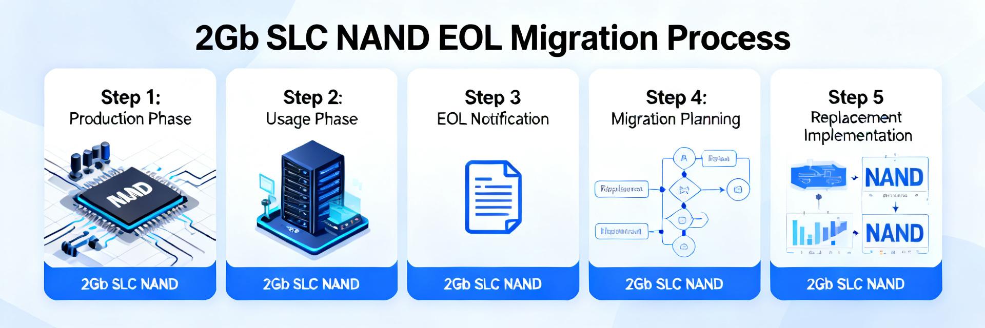
    The MT29F2G08ABAEAH4-IT:E is a 2 Gbit SLC NAND device targeted at industrial embedded applications; this guide confirms its key electrical and physical specs, interprets current EOL posture, and gives a pragmatic lifecycle playbook for engineers facing supply transitions. Sources used for validation include the official device datasheet, published lifecycle notices, distributor lifecycle flags, and community validation notes from field engineering—this document synthesizes those inputs into action items. The guide’s goals are fourfold: confirm spec-level details for fast engineering reference, interpret product-status and EOL signals, assess design and procurement impact, and present migration and lifecycle actions (last-time-buy, validation, and governance). Follow the checklists and matrices below to move from reconnaissance to an executable plan with clear owners and timelines. 1 — Product overview & key specs (background) MT29F2G08ABAEAH4-IT:E is a 2 Gbit SLC NAND organized as 256M x8 and intended for industrial temperature ranges; the part is commonly used where SLC NAND endurance and retention are required for deterministic embedded storage. The paragraph below and the compact spec table present fields engineers reference daily; confirm the exact datasheet revision before final BOM updates. — Electrical & physical specifications (what to list) Parameter Value (engineer quick ref) Density / Organization 2 Gbit (256M x8) I/O Voltage 3.3 V (industrial single-supply) Bus Width x8 (parallel NAND) Package / Ball‑Pin Count TSOP‑48 / 48 pin (confirm datasheet) Operating Temperature -40 °C to +85 °C (industrial) Page Size 2048 B main + 64 B spare Pages per Block 64 Block Size 128 KB Total Blocks 2048 (approx, based on 2 Gbit) ECC / ONFI Host ECC expected; ONFI support varies—confirm in datasheet — Performance, endurance & reliability metrics Key performance and reliability figures for design decisions include typical program latency, erase latency, maximum interface rate, P/E cycle endurance, and data-retention expectations. Typical SLC program times are sub-millisecond ranges and erase times a few milliseconds; industrial SLC endurance is commonly rated for tens to hundreds of kilocycles (P/E). For production, validate read/write timing, power use under load, and retention against your thermal profile. 2 — EOL status & lifecycle timeline (data analysis) To assess EOL for MT29F2G08ABAEAH4-IT:E, collect manufacturer lifecycle codes and cross-check published lifecycle pages and notices; distributor lifecycle flags and last-time-buy announcements provide corroborating signals. EOL interpretation requires recording status code, notice date, announced last-time-buy deadline, and suggested replacements in a dedicated log to support procurement decisions. HOST MCU / CONTROLLER MT29F2G08ABAEAH4 2Gbit SLC (TSOP-48) 3.3V x8 Parallel Bus Control (CLE, ALE, CE#, WE#, RE#) I/O Bus [7:0] VCC (3.3V) / GND — How to verify EOL status (practical checks) Verification checklist fields: lifecycle status code (active/obsolescence/end-of-life), date posted (notice timestamp), last-time-buy deadline, production discontinuation date, datasheet revision, and replacement recommendations. Operational checks: archive prior datasheet PDFs, capture distributor “lifecycle” flags, and save screenshots of notices. Keep a dated source log (datasheet rev and notice dates) for audit and release-control purposes. — Common EOL triggers & timeline patterns EOL triggers include process consolidation, low demand in legacy designs, and migration to higher-density or multi-level NAND types. Typical timelines run from announcement to discontinuation over several months to a year; last-time-buy windows can be short. Log milestones—announcement, last-time-buy, final ship—and apply conservative buffer months for critical systems to avoid field shortages. 3 — Impact analysis on designs & systems (data analysis / method) SLC NAND devices like this one affect long-term serviceability, firmware behavior, and BOM risk. Use the following risk matrix and test-focused compatibility checks to prioritize actions by severity and likelihood, and to decide between last-time-buy or redesign strategies. — Risk matrix for hardware & BOM Risk Area Severity Likelihood Mitigation Owner Supply shortage High High Last-time-buy; multi-sourcing Procurement Warranty / returns Medium Medium Stock spares; extended inspection QA Temperature/regulatory Medium Low Qualification testing Engineering Long-term maintenance High Medium Documented migration path Product mgmt — Technical compatibility risks (pinout, interface, firmware) Compatibility risks include package pinout differences, voltage/timing mismatches, and controller-level ECC differences that break boot or storage stacks. Recommended minimum tests: signal integrity (SI) checks, power/thermal profiling under worst-case load, and in-circuit boot validation. Suggested timeline: prototype integration (2–4 weeks), full validation (4–8 weeks), production sign‑off (2 weeks), adjusted to project scale. 4 — Replacement & migration strategies (method guide) When a drop-in replacement exists, match density, geometry, and electrical specs; otherwise plan firmware/controller adaptation or PCB changes. Use a decision tree approach: drop‑in candidate → firmware tweak → PCB change → redesign. For each step, document firmware impacts and regression tests required to reach parity with the incumbent SLC NAND behavior. — Finding direct replacements & compatibility checklist Replacement checklist: match I/O voltage and bus width, page/spare geometry, pages-per-block and total-block mapping, ECC/ONFI compatibility, and thermal/package mechanical fit. If a true drop-in is unavailable, evaluate adapter options or controller firmware that masks geometry differences. Use the long-tail search term MT29F2G08ABAEAH4-IT:E replacement as part of supplier queries and cross-reference candidate datasheets. — Firmware, controller & validation checklist Validation items: ECC configuration, wear-leveling and bad-block management, bootloader compatibility, regression test suites, and a field update plan. Provide a validation matrix with pass/fail criteria and estimate engineering effort per path: drop-in candidate (~40–80 hours), firmware tweak (~120–240 hours), PCB redesign (~240–480 hours), full product redesign (project dependent). 5 — Procurement & lifecycle management action plan (action) For MT29F2G08ABAEAH4-IT:E EOL handling, combine immediate procurement plays with long-term governance. Immediate actions secure runtime continuity; long-term policies reduce future exposure. Record actions with dates, owners, and urgency levels to convert analysis into procurement moves. — Short-term procurement playbook (urgent actions) Urgent checklist: confirm remaining certified stock, determine last-time-buy deadlines, place sample and production last-time-buy orders as prioritized by criticality, verify traceability and packaging, and flag BOM entries with EOL status and recommended replacement. Prioritize systems that cannot tolerate field updates and those with long lead validation needs. — Long-term lifecycle governance & design policy Recommended governance: formalize multi-sourcing and a qualified-alternative list, schedule periodic lifecycle reviews with a 24–36 month forecast horizon, and assign cross-functional owners (engineering, procurement, QA) with a quarterly review cadence. Embed contractual safeguards (supply commitments, last-time-buy terms) where possible for high-risk components. Summary MT29F2G08ABAEAH4-IT:E is a 2 Gbit SLC NAND (256M x8) with industrial temperature rating and standard 2KB page geometry; confirm exact package and ONFI support against the current datasheet before finalizing BOM decisions. The device shows classic EOL signals—manufacturer lifecycle notices and distributor flags—so immediate actions should include inventory verification, prioritized last-time-buy evaluation, and capturing notice dates and deadlines in a lifecycle log. Mitigation: perform quick compatibility checks, plan engineering validation (SI, power, firmware), and adopt governance (multi-sourcing, review cadence) to reduce future EOL exposure and maintain service continuity. Frequently Asked Questions What are the definitive MT29F2G08ABAEAH4-IT:E datasheet items to confirm before a last-time-buy? Before placing last-time-buy orders, confirm datasheet revision, exact package type and mechanical drawing, operating temperature spec, page/spare geometry, pages-per-block, total blocks, I/O voltage, and any ONFI or timing parameters that affect your controller. Record the datasheet revision and notice date in your procurement log to support future audit and qualification. How do I evaluate whether to buy spares or redesign for MT29F2G08ABAEAH4-IT:E EOL? Score parts by criticality: systems that cannot tolerate field replacement or extended downtime should trigger last-time-buy. Use the risk matrix to score severity and likelihood, estimate validation hours for replacement paths, and weigh inventory carrying costs vs. redesign effort. For critical units, last-time-buy + parallel migration plan is typical. What minimal validation is needed if replacing MT29F2G08ABAEAH4-IT:E with a candidate SLC NAND? Minimal validation: verify pinout and power rails, run SI checks at expected clock rates, validate controller ECC and bad-block handling with stress patterns, perform thermal/power profiling, and run a two-week system-level burn-in with real workloads. Pass/fail criteria should be defined in the validation matrix before production sign-off. What are the key technical specifications of MT29F2G08ABAEAH4-IT:E? The MT29F2G08ABAEAH4-IT:E is an industrial-grade 2 Gbit (256M x8) SLC NAND flash operating at 3.3V inside a TSOP-48 package. It supports temperature ranges from -40°C to +85°C, with a page size of 2048B + 64B spare, and requires host controller ECC integration.
  • MT41K512M16VRP-107 IT:P datasheet: key specs & tests

    Point: The MT41K512M16VRP-107 IT:P is an 8 Gbit DDR3L-class automotive-grade device with a 933 MHz effective data rate at 1.35V operation, and engineers routinely consult the MT41K512M16VRP-107 IT:P datasheet for verification of thermal, timing and qualification limits. Evidence: The official part description lists twin-die x16 organization targeted for automotive/high-reliability systems. Explanation: This article breaks the datasheet into actionable specs, test guidance and an integration checklist to accelerate design and qualification. Point: Purpose is practical and data-driven: isolate the must-check electricals, timing margins and board-level rules that determine success in infotainment, ADAS buffers and logging units. Evidence: Datasheet tables contain the authoritative timing and package constraints used during design reviews. Explanation: Engineers using this guide will know which datasheet fields to prioritize during bench validation and PCB layout. 1 — MT41K512M16VRP-107 IT:P — part overview & package (background) — Device family & functional summary Point: The device is a DDR3L-style 8 Gbit memory arranged as two x8 dice to present a x16 device width, with nominal VDD/VDDQ = 1.35V and automotive qualification variants. Evidence: The datasheet summarizes density, operating voltage and target applications (automotive/high-reliability). Explanation: For system architects, this means the device supports typical DDR3L timing stacks and requires controller setup for x16 width and the twin-die behavior when calculating bank interleaving and burst characteristics. — Package, pinout & mechanical notes Point: Package is an FBGA with a specified ball count and footprint; mechanical drawings in the datasheet define body dimensions, ball pitch and recommended land pattern. Evidence: Datasheet mechanical diagrams give pad size, PCB solder-mask recommendations and thermal via placement guidance. Explanation: Follow the datasheet land pattern and thermal recommendations exactly—incorrect pad size or missing thermal vias under the FBGA are common causes of assembly defects and thermal derating in automotive environments. Quick spec summary Parameter Value Density 8 Gbit (x16 twin-die) Nominal VDD / VDDQ 1.35 V Effective data rate 933 MHz (DDR3L class) Package FBGA (specified ballout) 2 — Key electrical specs for MT41K512M16VRP-107 IT:P (data analysis) — Power rails, I/O voltage ranges & current consumption Point: Key electrical specs: VDD/VDDQ nominal 1.35V with allowed tolerances; I/O voltage must follow datasheet limits and power-sequencing requirements. Evidence: The datasheet lists typical active, precharge and self‑refresh currents and the ΔI differences across modes. Explanation: Validate both typical and worst-case currents during qualification—self‑refresh and standby leakage can drive thermal and battery impact in automotive systems, so include margin for tolerance and part-to-part variation. Mode vs typical current (example) Mode Typical current Active (read/write) ~150–250 mA (device dependent) Precharge/Standby ~20–50 mA Self‑refresh ~5–15 mA — Operating frequency, data rate & timing overview Point: The device supports DDR3L-class effective rates (example 933 MHz effective), with CL and tCK ranges defined in the timing tables. Evidence: Datasheet timing summary shows supported CL values and required tRCD/tRP/tRAS windows at each data rate. Explanation: On-bench validation must reproduce datasheet timing points; controller firmware should be configured for the part's supported CL/tCK combos and validated for margin at temperature and voltage extremes. 3 — Memory organization & timing parameters (data deep-dive) — Bank/row/column architecture and addressing Point: Internal organization uses multiple banks and standard row/column addressing; the twin-die x8 composition presents as x16 to the controller, influencing burst and interleave behavior. Evidence: Datasheet memory map and address pin description define row/column/bank bit counts. Explanation: Map controller address lines and chip-select handling per the datasheet recommendation to avoid unintended bank conflicts and to maximize burst efficiency during sequential transfers. MT41K512M16VRP (Twin-Die) VDD/VDDQ (1.35V) ADDR/CMD CK / CK# DQ[15:0] DQS[1:0] / DQS#[1:0] VSS/VSSQ (GND) — Detailed timing table & practical notes Point: Validate tCK, CL, tRCD, tRP, tRFC and tWR at your target operating point; datasheet lists nominal values and temperature/voltage derating. Evidence: Timing table provides example tCK ranges and corresponding timing windows. Explanation: Use the datasheet as the baseline and then create bench test points at worst-case temperature and lowest allowed VDD to measure real margin; margin failures typically trace back to signal integrity or power delivery issues. Representative timing parameters Parameter Example tCK ~1.07 ns (for 933 MHz effective) CAS Latency (CL) 6–11 cycles (device dependent) tRCD / tRP ~13–16 ns (check datasheet) tRFC variable by density; validate per datasheet 4 — Recommended electrical & timing tests (method guide) — Required bench tests and test fixtures Point: Standard validation includes power sequencing checks, JEDEC ID reads, read/write data integrity at target speeds and retention/refresh tests. Evidence: Datasheet sections on power sequencing and AC/DC tests define required limits. Explanation: Use a DDR protocol-aware DVT tool for read/write stress, verify JEDEC register values, run retention at temperature extremes and include repeated power‑cycle tests to reveal marginal parts or layout problems. — Signal integrity & timing validation Point: SI tests should include eye-diagram capture, jitter measurement and worst-case skew verification across address/command nets. Evidence: Datasheet timing margins and recommended termination schemes establish acceptable windows. Explanation: Capture eyes at the controller and DRAM pins; use pass/fail criteria defined from datasheet timing plus a designer margin (typically 10–20%) to decide if layout or termination changes are needed. Test matrix (example) Test Equipment Pass/Fail Power-sequence Bench PSU, scope Meets VDD ramp & sequencing limits Read/Write at target rate DDR DVT tool, LA No data errors for 24h burn SI eye test High-speed scope, BERT Eye opening ≥ datasheet margin 5 — Integration & PCB design guidelines (method guide) — Footprint, thermal, and power-delivery recommendations Point: Follow recommended land pattern, include thermal vias and implement a disciplined decoupling strategy close to VDD/VDDQ pins. Evidence: Datasheet mechanical and power recommendations indicate bypass placement and via locations. Explanation: Place high-frequency decoupling within 5 mm of device power pins and use multiple bulk and ceramics per the datasheet to stabilize VDD during bursts. — Routing, termination, and routing topology Point: Adhere to matched-length routing for address/command nets, and choose fly‑by or T‑topology per the system memory architecture. Evidence: Datasheet timing tolerances and suggested termination schemes inform topology choices. Explanation: For single-rank designs prefer fly‑by with proper point-of-load termination; in multi-drop scenarios, manage stub lengths and use series termination to preserve timing margins (target 100–200 ps skew budget). 6 — Performance benchmarks, use cases & qualification checklist (case + action) — Typical performance metrics & example use cases Point: Expect sustained sequential throughput in the hundreds of MB/s per interface depending on controller and system topology; random latency follows CL and tRCD tradeoffs. Evidence: Datasheet timing and bandwidth figures define theoretical maxima. Explanation: Map these metrics to use cases: infotainment streaming benefits from high sequential throughput, ADAS buffering requires low-latency deterministic behavior and logging workloads favor sustained write robustness. — Qualification checklist & production test pointers Point: Qualification should include datasheet compliance, automotive stress tests (temp/voltage cycling, ESD, retention) and lot acceptance sampling with defined sample sizes. Evidence: Datasheet notes on temperature ranges and electrical compliance set baseline requirements. Explanation: Maintain a checklist: verify part-number suffixes for temperature/qualification variants, re-check datasheet revision on every PO, and run full electrical and SI validation before production sign-off. Summary Reference the official datasheet for authoritative MT41K512M16VRP-107 IT:P specs and package drawings before layout or purchase decisions. Prioritize power-sequencing, SI eye margin capture and timing validation at worst-case VDD/temperature to meet automotive reliability. Implement recommended decoupling, thermal vias and matched routing; validate with DDR protocol DVT tools and make layout changes based on measured margin failures. FAQ What are the critical timing checks for MT41K512M16VRP-107 IT:P? Check tCK, CL, tRCD, tRP, tRFC and tWR at worst-case voltage and temperature. Run read/write stress at target data rates and capture eye diagrams; its datasheet timing table provides the baseline values to compare against measured margins. How should I test power sequencing for MT41K512M16VRP-107 IT:P? Use a controlled bench PSU to exercise VDD and VDDQ ramps against the datasheet sequencing window, verify JEDEC ID after each cycle, and include repeated power cycles in qualification to reveal latent assembly or layout issues. What PCB layout items from the datasheet are most likely to fix margin failures for MT41K512M16VRP-107 IT:P? Prioritize correct land pattern, thermal vias under the FBGA, close decoupling (within ~5 mm), dedicated power planes and matched-length address/command routing; these changes address the majority of SI and power-related margin failures. Why is the MT41K512M16VRP-107 IT:P classified as a twin-die device, and how does it affect layout? The device package integrates two x8 dice wired in parallel to achieve a x16 width. This structure shares address lines but increases input capacitance, requiring strict adherence to datasheet-specified loading margins and trace length matching.
  • MT25QL256ABA8E12-1SIT Datasheet: Key Specs & Pinout

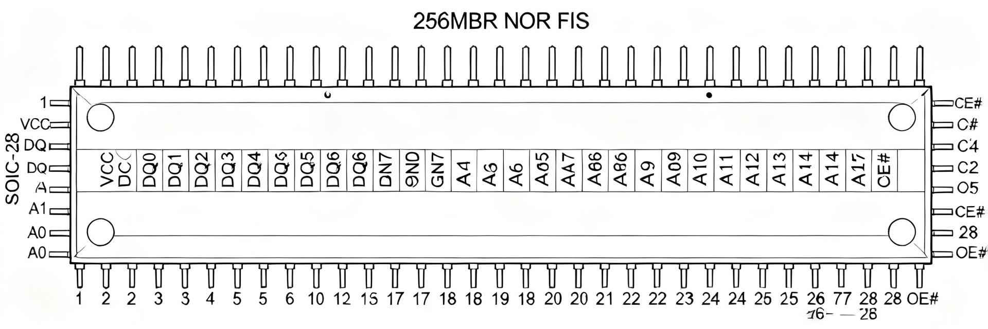
    The MT25QL256ABA8E12-1SIT is a 256‑Mbit serial NOR flash device with high‑speed I/O, commonly rated for up to 133 MHz clock operation; this combination makes it a frequent choice for firmware storage and boot ROM in embedded systems. This article gives you a concise reference of key specs, full pinout guidance, interface tips, and a practical implementation checklist—consult the official datasheet for absolute values and revision details. You will find focused sections: background and typical uses, electrical and performance highlights, a clear pinout table, interface/command guidance, plus PCB layout and debug steps. Treat the manufacturer datasheet as the source of truth for precise timing, current values, and package drawings before production or qualification. 1 — Background: What the MT25QL256ABA8E12-1SIT Is 1.1 Device class & common applications Point: This part is a serial NOR flash memory device that supports SPI and higher‑I/O modes. Evidence: The device class and quad I/O capability are documented in the official materials. Explanation: You’ll typically use it for firmware and boot storage, LUTs, configuration blobs, and small file systems in IoT, consumer electronics, and embedded controllers where random‑read and execute‑in‑place are valuable. 1.2 How to use the datasheet as source of truth Point: The datasheet is the authoritative reference for electrical, timing, pin descriptions and mechanical drawings. Evidence: Key sections to prioritize are electrical characteristics, pin descriptions, timing diagrams, and the command set. Explanation: When you quote voltages, currents, or opcodes for production, cross‑check revision numbers and page figures in the official datasheet to avoid mistakes in implementation and procurement. 2 — Key Electrical & Performance Specs Parameter / Feature Specification Details Memory Capacity 256 Megabit (32 Megabytes) Supply Voltage (VCC) 1.7V to 2.0V Range (1.8V Nominal) Max Clock Frequency Up to 133 MHz (Single / Quad I/O Modes) Erase Granularity 4KB Subsector, 64KB Sector, Bulk Erase Data Retention 20 Years (Typical at System Operating Temperature) 2.1 Memory organization, capacity, and endurance Point: The device provides 256 Mbit total capacity organized into bytes and conventional pages and blocks. Evidence: The datasheet lists total bits/bytes, page sizes, sector/block erase granularity, program/erase endurance cycles, and data retention guarantees. Explanation: For example, you should map firmware images to page and sector boundaries, plan erase cycles per block within endurance limits, and confirm retention specs for your product lifetime. 2.2 Power, timing, and performance highlights Point: Expect a specified VCC range, operating currents for read/program/erase, and a maximum clock near 133 MHz. Evidence: Datasheet tables differentiate typical vs. max currents, list I/O timing parameters (tCH, tCL, tCS), and note different values for STR, DTR or quad modes. Explanation: Use the compact timing table for clocking decisions, and plan for low‑power standby values and any mode‑specific current increases during program/erase. 3 — Pinout & Package Details MT25QL256ABA NOR FLASH S# (CS#) DQ0 / SI DQ1 / SO VCC C (CLK) VSS (GND) 3.1 Pin mapping: functional pin table Point: The pinout assigns pins for IO0–IO3, SCK, CS#, power and ground; some pins are active‑low control signals. Evidence: Typical functional names include IO0 (SI), IO1 (SO), SCK (clock), CS# (chip select), WP# (write protect) and HOLD#; power pins carry VCC and multiple GND pins for thermal/current return. Explanation: Review the pinout table carefully to wire CS#, WP# and HOLD# correctly, tie unused inputs per the datasheet, and respect IO voltage domains to avoid latch‑ups. 3.2 Package drawing, footprint and mechanical notes Point: Multiple package variants and mechanical dimensions are provided; footprint guidance is critical. Evidence: Mechanical drawings specify pad layout, recommended solder mask openings, pad dimensions, pin‑1 indicator and board keepouts. Explanation: When you design the footprint, follow the recommended pad sizes, add solder mask clearance, mark pin‑1, and include thermal/ground vias as advised to ensure solderability and thermal performance. 4 — Interface Modes, Commands & Timing Diagrams 4.1 SPI / Quad I/O modes and common commands Point: The device supports single‑SPI and multi‑I/O modes and a compact command set for read, program, erase and status operations. Evidence: Common opcodes include Read (and Fast Read variants), Page Program, Sector/Block Erase, Read ID, Write Enable/Disable, and Reset. Explanation: In practice, implement a minimal command subset for bring‑up (Read ID, Read, Write Enable, Page Program, Erase), and consult the datasheet opcode map for full command lengths and expected response bytes. 4.2 Timing diagrams and example sequences Point: Key sequences are read, page program and erase flows with CS# toggling and address phases. Evidence: Timing diagrams in the datasheet show clock polarity/phase, command/address/data windows, and required delays between operations. Explanation: A typical sequence is CS# low → opcode + address → data transfer → CS# high; use the specified clock phase/polarity and required inter‑command delays, and capture signals with a logic analyzer to validate timing during bring‑up. 5 — Design, Layout & Debug Checklist 5.1 PCB layout and power sequencing best practices Point: Proper decoupling, short clocks, and clean ground routing directly affect reliability. Evidence: Recommended practices include placing decoupling caps close to VCC pins, using star or plane grounds, and routing clock/IO traces short with series damping resistors if needed. Explanation: Place 0.1 μF and 1 μF decouplers near power pins, avoid long stub traces to the flash, and consider level shifters if the host MCU I/O voltage differs from the flash VCC. 5.2 Common failure modes and troubleshooting steps Point: Many failures stem from wiring, power, or timing mismatches. Evidence: Typical issues are incorrect pin mapping, missing decoupling, SPI mode mismatch, floating HOLD/WP, or signal integrity artifacts. Explanation: For debug, verify VCC and GND, toggle CS while capturing the bus with a logic analyzer, issue a Read ID as the first test, and inspect solder joints and footprint alignment if communication fails. Summary The MT25QL256ABA8E12-1SIT is a 256‑Mbit serial NOR flash suited for firmware and boot storage; consult the official datasheet for exact capacity, endurance and timing before production. Key electrical items: check VCC range, active/read/program currents, and max clock (near 133 MHz); align your firmware image to page/sector sizes listed in the datasheet. Use the pinout and package guidance when placing the footprint: follow pad sizes, pin‑1 marking, decoupling placement, and ground/thermal recommendations to avoid assembly and reliability issues. 6 — Common Questions What are the essential steps to validate MT25QL256ABA8E12-1SIT on a new board? Start by checking power rails and decoupling, confirm correct footprint and pin mapping, then issue a Read JEDEC/ID command with the chip selected. Use a logic analyzer to capture clock and IO lines; successful ID response and stable read transactions confirm basic communication before programming tests. How do you choose the right SPI mode and clock settings for MT25QL256ABA8E12-1SIT? Refer to the timing diagrams for required clock polarity and phase; begin with a conservative clock (e.g., a fraction of max) to validate signal integrity. Gradually increase clock to the device’s supported maximum while monitoring for CRC or read errors; select STR/DTR or Quad modes only after verifying electrical margins. What are the quickest troubleshooting steps when MT25QL256ABA8E12-1SIT fails to respond? Verify VCC/GND voltages, ensure CS# is asserted correctly, check HOLD#/WP# states, inspect solder joints, and capture SPI traffic. If you see no activity, reflow or check footprint alignment; if traffic is noisy, add series resistors and shorten traces. Finally, attempt a Read ID as an initial sanity check. How should the WP# and HOLD# pins be handled if they are not actively used? If WP# (Write Protect) and HOLD# (Hold) functions are not actively controlled by the host MCU, they should be pulled high to VCC through individual pull-up resistors (typically 4.7kΩ to 10kΩ). Leaving these inputs floating can lead to accidental write-protection or clock suspension, causing unpredictable device behavior.
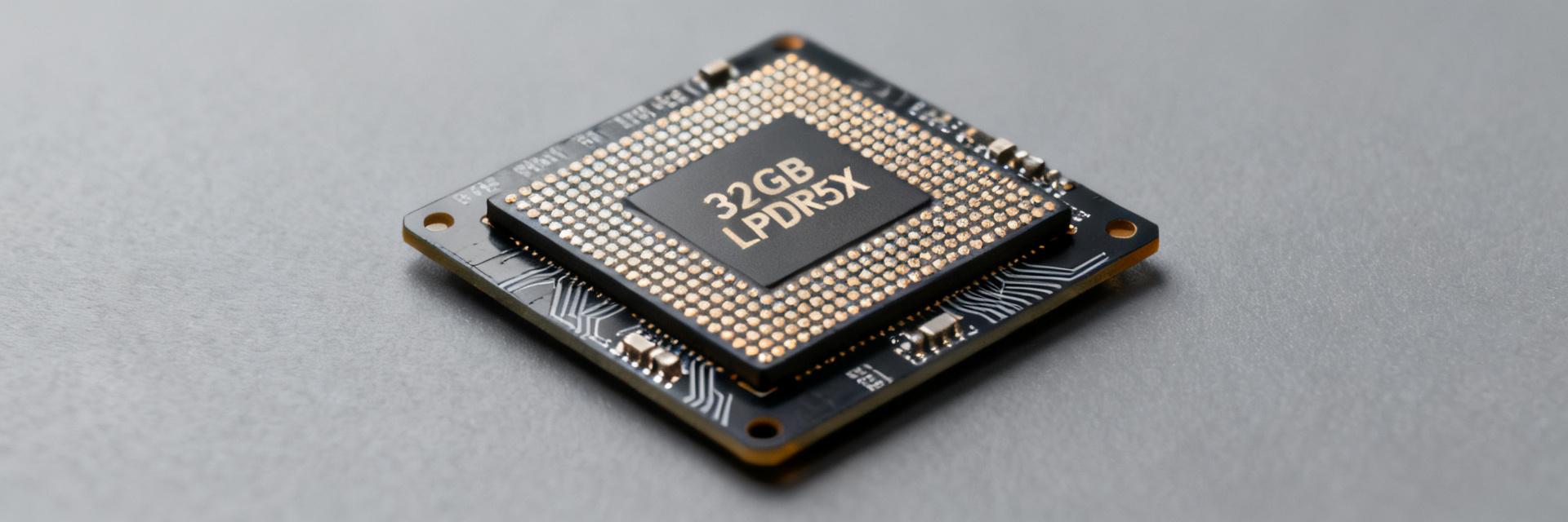
  • MT62F1G32D2DS-023 LPDDR5X Specs: Complete Datasheet Overview

    This guide unpacks the MT62F1G32D2DS-023 LPDDR5X datasheet and translates the key electrical, timing, package, and integration specs engineers need to design with this 32Gb-class LPDDR5X device. Point: Present headline numbers up front; Evidence: Datasheet tables list 32Gb density and high-bandwidth speed grades; Explanation: Readers can map those numbers to system bandwidth and integration risk quickly. Point: Article structure and reading order are pragmatic for bring-up. Evidence: The following sections move from device overview to electrical, performance, package, then a hands-on checklist. Explanation: Recommended reading order is Introduction → Device overview → Electrical/timing → Integration/performance → Package/thermal → Design checklist → Summary and FAQ for fast design-review use. Device overview & key features MT62F1G32D2DS-023 LPDDR5X x32 32Gb (4GB) VDD/VDDQ CK_t / CK_c WCK_t / WCK_c DQ[31:0] CA[6:0] VSS / GND Part numbers, density & speed grades Point: The device family covers a 32Gb density (4GB-equivalent) in x32 organization. Evidence: The datasheet part mapping table lists suffix variants tied to speed grades. Explanation: Use the table below to match suffix → density → peak data rate when choosing parts and listing long-tail keywords for procurement and BOM notes. Part suffix Density Max data rate (Mb/s per pin) -023 32Gb (4GB equiv.) 8533 -WT 32Gb (4GB equiv.) 7400 Core device features & standards support Point: Primary features include x32 bus, multi-bank architecture, low-power modes, and optional on-die features. Evidence: Datasheet feature checklist enumerates channel width, bank count, LPDDR5X low-power states, and training support. Explanation: Confirm JEDEC compliance rows and optional items (on-die ECC, enhanced training) in the datasheet to validate controller compatibility early. Electrical characteristics & timing Supply voltages, IO specs & power modes Point: Nominal core and I/O voltages and power-state currents drive decoupling and power-sequencing decisions. Evidence: The datasheet voltage tables list VDD, VDDQ ranges and dynamic/static current at defined data rates. Explanation: Use those table values to size regulators, place decoupling near VDD/VDDQ pins, and plan power sequencing with recommended topologies to limit inrush and droop. Timing parameters, data rates & bandwidth Point: Timing metrics (tCK, tRCD, CAS-like latencies) determine controller setup. Evidence: Timing tables provide tCK ranges and timing rows per speed grade; max listed data rate yields raw bandwidth. Explanation: Convert listed data rate to peak bandwidth by: bandwidth = data rate × bus width / 8. For x32 at 8533 Mb/s, peak ≈ 34.1 GB/s per device. Performance & system integration Calculating effective throughput & latency trade-offs Point: Theoretical peak differs from sustained throughput due to refresh, conflicts, and bursts. Evidence: Datasheet rates and timing rows define theoretical max; system-level models show refresh/row-hit effects. Explanation: Run sample calculations combining device peak bandwidth, x32 width, and realistic duty factors (for example 60–80% sustained) to size memory paths and expected latency. Controller/PHY configuration and signal integrity checklist Point: Correct PHY setup and SI practices prevent training failures. Evidence: Datasheet notes cover WCK/CK ratios, required training sequences and ODT recommendations. Explanation: Verify WCK/CK mode, training step ordering, termination values, impedance targets, and trace length matching during schematic and PCB review before first power-up to reduce bring-up iterations. Package, thermal & reliability considerations Package details, pinout & footprint guidance Point: The device uses a high-ball-count BGA-style package with tight land-pattern tolerances. Evidence: Mechanical drawings and pinout tables in the datasheet specify ball map and keepout dimensions. Explanation: Extract critical dimension rows, verify land pattern, and prioritize routing for power/ground, clocks and command/address lanes while reserving keepout areas for thermal vias. Thermal limits, operating ranges & qualification notes Point: Operating temperature and junction limits set derating and thermal mitigation needs. Evidence: The datasheet lists operating temperature ranges, Tmax junction and recommended thermal suggestions. Explanation: Derive PCB copper, thermal via arrays and possible heatsinking from those numbers and confirm qualification (JEDEC/AEC notes) for your target application and environmental tests. Design checklist & practical validation steps Schematic, power sequencing & PCB routing checklist Point: A prioritized checklist prevents common schematic/PCB errors. Evidence: Datasheet sections define recommended sequencing, decoupling placement and WCK/CK routing. Explanation: Enforce power order, place decoupling within millimeters of VDD pins, use star routing for supplies, match WCK/CK pairs, and validate ODT and termination values in schematic notes before layout sign-off. Firmware/bring-up & validation plan Point: A staged bring-up plan reduces risk and isolates faults. Evidence: Protocol training flow and PHY calibration sequences are described in the datasheet training notes. Explanation: Begin with power and continuity checks, then run JEDEC training, PHY calibration, stress patterns and timing margin sweeps; collect pass/fail criteria for latency, throughput and bit-error-rate under thermal stress. Summary - Key takeaways Confirm part-suffix to density and speed mapping from the datasheet before BOM freeze; this ensures correct MT62F1G32D2DS-023 speed grade selection and controller timing targeting. Size regulators and decoupling from the listed VDD/VDDQ ranges and dynamic/static currents; place decoupling close to power pins and plan power sequencing per datasheet notes. Convert listed data rate to peak bandwidth with bandwidth = rate × bus width ÷ 8 and plan sustained throughput at 60–80% of peak to account for refresh and bank conflicts. Frequently Asked Questions What are the essential voltage ranges in the MT62F1G32D2DS-023 LPDDR5X datasheet? Point: Knowing nominal and allowable voltage ranges avoids damage and timing shifts. Evidence: Voltage tables specify VDD and VDDQ nominal and min/max limits. Explanation: Use those ranges to pick regulators with margin, implement power sequencing rules, and verify decoupling to keep transient excursions within specified limits during high-rate transfers. How do I convert the datasheet data rate to system GB/s for x32 devices? Point: Conversion is straightforward and critical for bandwidth budgeting. Evidence: The datasheet lists max data rate in Mb/s per pin for each speed grade. Explanation: Apply bandwidth = data rate × 32 ÷ 8; for an 8533 Mb/s grade the peak device bandwidth ≈ 34.1 GB/s, then factor realistic duty cycle for sustained throughput. Which checklist items in the datasheet are most often missed during bring-up? Point: Common misses are sequencing, termination and training order. Evidence: Datasheet recommended sequencing, ODT notes and training steps are explicit. Explanation: Double-check power-up order, ODT and termination values, WCK/CK routing and length matching, then run the prescribed training sequences immediately after powering to avoid elusive timing and SI failures. What are the primary differences between the -023 and -WT speed grades? Point: The main distinction lies in maximum bandwidth performance parameters. Evidence: The speed grade lookup tables in the datasheet map -023 to a peak of 8533 Mb/s per pin and -WT to 7400 Mb/s per pin. Explanation: Design engineers should utilize the -023 speed grade when designing for peak performance applications and the -WT speed grade for mainstream bandwidth layouts.
  • MT41K256M16TW-107 DDR3L: Complete Specs & Pinout Guide

    The MT41K256M16TW-107 is a 4 Gbit device organized as 256M × 16 in a 96-ball FBGA, optimized for low-voltage DDR3L operation at 1.35 V and capable of DDR3-1866 timing (effective 933 MHz I/O). These parameters directly affect power budget, board area, and achievable throughput—critical factors for mobile and thermally constrained designs. This guide delivers a PCB-ready pinout checklist, concise electrical highlights, and practical routing and verification tips designers can apply during schematic capture, layout and lab bring-up without referencing vendor pages—use the official manufacturer datasheet for exact component tables during final sign-off. 1 — Product Overview & Architecture 1.1 — Memory Organization & Capacity The device presents 4 Gbit total capacity as 256M × 16 data width with internal bank partitioning (multiple banks and selectable bank-address bits). Host controllers see linear addresses mapped to row/column/bank fields; software and memory controller configuration must match the device's row/column sizing to ensure correct addressing and refresh behavior for full capacity utilization. 1.2 — Voltage & Power Modes Rated for 1.35 V nominal VDD/VDDQ, the part supports standard DDR3L low-voltage operation including active, precharge, and self-refresh low-power states. Using DDR3L reduces DRAM power by tens to hundreds of milliwatts in typical mobile profiles, improving battery life and easing thermal constraints in compact systems compared with traditional 1.5 V DDR3 devices. 2 — Key Electrical Specifications 2.1 — Speed Grades & Timing Parameters Selected speed grade supports up to a 933 MHz I/O effective rate (DDR3-1866 timing). Designers should reference tCK, CAS latency (CL), tRCD, tRP and tRAS values for the chosen timing point and set controller training margins accordingly. MT41K256M16TW-107 timing choices influence route length budgets and signal integrity requirements on the PCB. 2.2 — Power, Thermal & Reliability Metrics Typical active and standby currents vary by access pattern; expect higher VDD/VDDQ currents during sustained reads/writes and much lower currents in self-refresh. Design PDN to handle peak active currents plus margin, monitor die temperature with thermals on critical boards, and verify JEDEC-compatible reliability parameters using the manufacturer datasheet before final approval. Electrical snapshot Parameter Representative value Density / Organization 4 Gbit (256M × 16) Nominal VDD / VDDQ 1.35 V (DDR3L) Max I/O rate 933 MHz effective (DDR3-1866 timing) 3 — Pinout & Package Details 3.1 — Package Type, Ball Count & Mechanical Notes The part comes in a 96-ball TFBGA/FBGA package with a tight ball pitch and compact footprint; follow the recommended land pattern from the official mechanical drawing during PCB library creation. Pay attention to reflow profile recommendations and handling notes to prevent warpage; include a properly dimensioned courtyard and thermal vias if the datasheet suggests a center expose pad. 3.2 — Signal Groups & Ball Mapping Group and label power clusters (VDD/VSS), DQ[0:15] and associated DQS/DQS# strobes, address lines A[0:N], bank address BA0–BA2, command pins RAS/CAS/WE, differential clocks CK/CK#, CKE, ODT, RESET#, and VREF. The pinout schematic map is represented in the diagram below to aid accessibility and layout capture. MT41K256M16TW-107 96-ball FBGA (DDR3L) CK / CK# A[14:0] / BA[2:0] RESET# VREF DQ[15:0] DQS[1:0] / DQS#[1:0] VDD / VSS VDDQ / VSSQ 4 — Timing, Signal Integrity & Routing Guidelines 4.1 — Clocking, Termination & Impedance Control Route CK/CK# as tight differential pairs with controlled 100 Ω differential or 50 Ω single-ended reference impedance per board stack-up. Use manufacturer-recommended RTT termination settings implemented near the controller or the DRAM as appropriate; place VREF decoupling next to VREF ball clusters to stabilize reference for on-die termination behavior. 4.2 — Data Strobe, Fly-by Topology & Length Matching Implement fly-by topology for address/command with series termination at the controller and short stub connections to each rank. For DQ/DQS use source-synchronous routing with DQS capture timing in mind—match DQ-to-DQS within each byte lane and keep skew budgets tight; limit stub lengths and adhere to the controller's recommended maximum trace lengths. 5 — PCB Integration Checklist & Example Schematic Notes 5.1 — Power Delivery & Decoupling Strategy Place high-frequency decoupling capacitors (0.01–0.1 μF) and bulk caps near VDD and VDDQ ball groups; follow the datasheet suggested capacitor mix and place them on the component side within a few millimeters of the balls. Verify PDN with impedance targets and run power sequencing checks to respect VDD/VDDQ ramp order during bring-up. 5.2 — Example BOM, Layout Tips & Verification Steps Typical BOM includes appropriate capacitor values, small series resistors for data lines if required, and 0 Ω or ferrite for power routing. Layout guidance: keep command/address runs short and straight, cluster decoupling near the device, and place termination near the source. Verify with IBIS/SPICE models and run DDR training and margin tests in the lab. 6 — Common Issues, Troubleshooting & FAQs 6.1 — Typical Failure Modes & Diagnostic Flow Common failures: training failures, marginal eye due to SI, incorrect VREF or RTT settings, and address parity errors. Triage by first validating power rails and VREF, then capturing clock and data with a high-speed scope during DDR training. Progress to controlled timing sweeps and termination adjustments to isolate root causes quickly. 6.2 — Quick FAQ & Selection Advice Choose x16 when system bus efficiency and higher width matter; x8 parts provide routing flexibility for multi-rank configurations. Single-rank designs simplify timing and routing; multi-rank increases capacity but tightens signal integrity constraints. Compare density, voltage, and package footprint to match your board's PDN and thermal budgets. Summary The device offers 4 Gbit capacity arranged as 256M × 16 with low-voltage DDR3L operation at 1.35 V, and requires disciplined pinout, termination and routing practices to achieve reliable DDR3-1866 performance. Prioritize correct VREF/RTT settings, clustered decoupling, and byte-lane length matching for a predictable bring-up. Reference the official datasheet and pinout PDF early and execute the verification checklist before tape-out. Key Takeaways MT41K256M16TW-107 provides compact 4 Gbit DDR3L density useful for space-constrained designs; verify addressing and controller settings to map the 256M × 16 organization correctly. Low-voltage DDR3L (1.35 V) reduces power and thermal load; implement recommended PDN decoupling and monitor VDD/VDDQ during active workloads. Pinout and routing priorities: group power pins, stabilize VREF, route CK/CK# as controlled differential pairs, and match DQ/DQS lengths per byte lane for robust signal integrity. Frequently Asked Questions Is MT41K256M16TW-107 suitable for low-power mobile applications? Yes—its DDR3L 1.35 V operation lowers active and standby power relative to 1.5 V parts. Combine careful PDN design and appropriate low-power modes (self-refresh during suspend) to maximize battery life; validate idle and active current in a representative system to confirm expected savings. What are the most important pinout considerations for layout? Prioritize grouping VDD/VSS clusters and placing decoupling close to power balls, mark NC/test balls clearly, provide a solid reference plane under CK/CK#, and annotate DQ/DQS pairs in the pinout so layout engineers can enforce byte-lane matching and keep stubs minimal for reliable timing margins. Which lab checks should be performed after layout to validate DDR3L integration? Run DDR controller training, capture eye diagrams on read/write operations, sweep address/command timing margins, validate VREF and termination settings, and perform write/read margin tests across temperature and voltage corners. Use IBIS/SPICE simulations and real silicon training logs to iterate until margins meet target specifications. What is the significance of the DDR3-1866 speed grade for this device? The DDR3-1866 timing capability supports up to a 933 MHz I/O clock (1866 MT/s effective data rate). This high-speed performance requires precise trace length matching, strict 50-ohm single-ended / 100-ohm differential impedance control, and optimized ODT settings to ensure clean signal transitions and adequate margin.
  • DDR3L 4Gb Parts Breakdown: Specs, Pinouts & Benchmarks

    Point: DDR3L 4Gb remains a practical choice for legacy laptops, embedded modules and cost-sensitive designs due to its low-voltage 1.35V footprint and wide availability. Evidence: System-level power budgets and module inventories frequently show DDR3L as the common low-voltage option for single-rank SODIMMs and soldered-down arrays. Explanation: This article delivers clear DDR3L 4Gb specs, pinout guidance and practical benchmark recommendations to help engineers and technical buyers select and validate parts efficiently. Point: Readers should expect actionable device organization notes, electrical basics, benchmark methodology and bench-to-production checklists. Evidence: Each section synthesizes typical datasheet parameters, package pin maps and measurement points used in qualification labs. Explanation: Follow the sections in order to translate device density into module capacity, assess performance by speed grade, and validate parts from prototype to production. DDR3L 4Gb — architecture & core specs (Background) Density, organization & addressing (x4 / x8 / x16) Point: "4Gb" denotes four gigabits per device and organization determines the data bus width and how many devices produce a given module capacity. Evidence: Typical organizations for 4Gb parts are 256M x16 or 512M x8 (logical equivalence), with bank and row/column addressing shown in manufacturer datasheets. Explanation: Translate device count to module bytes by summing device widths per rank (e.g., eight x4 devices yield a x32 data path); use organization to plan rank/channel topology for the memory controller. Configuration Addressing Structure Bank Count Page Size 512M x 8 16 Rows x 10 Columns 8 Banks 1 KB 256M x 16 15 Rows x 10 Columns 8 Banks 2 KB Voltage, timing & electrical basics (1.35V, CL, data rates) Point: DDR3L nominally operates at 1.35V with standard DDR3 timing parameters directly affecting throughput and latency. Evidence: Speed grades commonly follow MT/s labels such as 1066, 1333, 1600 and 1866, and timing metrics include CAS latency (CL), tRCD, tRP and tRAS on datasheets. Explanation: Lower VDD reduces active and standby power; choose a speed/timing trade-off (lower CL at a given MT/s yields better latency) aligned with controller timing tables and system thermal budget. (Use DDR3L specs from the device datasheet to set controller registers.) Performance benchmarks & electrical behavior of DDR3L 4Gb (Data analysis) Throughput, latency and bandwidth across speed grades Point: Bandwidth scales with MT/s and channel width while latency depends on CAS cycles and tCK; single-rank vs dual-rank affects effective throughput under real workloads. Evidence: A single 64-bit channel at DDR3-1600 (1600 MT/s) yields theoretical peak bandwidth of 12.8 GB/s per channel; rank interleaving and wider channels raise sustained throughput in streaming tests. Explanation: Run sequential and random microbenchmarks to observe how rank count and interleaving impact real-world patterns, and compare latency numbers (ns) by converting CL*tCK for apples-to-apples comparisons. CMD/ADDR BUS CK / CK# DDR3L 4Gb Memory Array 8 Banks (512M x 8 / 256M x 16) Data / Power DQ / DQS VDD/VDDQ (1.35V) | VSS (GND) Power draw and thermal considerations (1.35V benefits) Point: Operating at 1.35V reduces dynamic power roughly proportional to V^2 and lowers thermal dissipation in tightly packed systems. Evidence: Measured active current decreases when moving from 1.5V to 1.35V; idle power also drops due to lower termination and device standby levels. Explanation: Target VDD/VDDQ measurement points on populated modules during idle and heavy access, and account for Vref stability and board-level heat spread when planning mobile or embedded thermal solutions. Pinout & package guide for 4Gb DDR3L devices (Method guide) Common package pinouts: FBGA, TSOP and what to watch for Point: 4Gb DRAM appears in FBGA and TSOP packages with pin assignments for clocks, data strobes and command/address that demand careful layout. Evidence: Datasheet package diagrams identify CK/CK#, DQ/DQS pairs, CA bus, Vref, VDD and VSS locations and recommended decoupling near VDD pins. Explanation: Prioritize matched-length DQ/DQS routing, close decoupling on VDD/VDDQ, and clear return paths for high-speed clocks to preserve signal integrity; consult the device 'pinout' section of the datasheet for exact maps. SODIMM module pinout notes & mechanical considerations Point: 204-pin SODIMMs group signals into predictable banks and include mechanical keying that affects module-to-board integration. Evidence: Module drawings lay out signal grouping by pin ranges and specify mechanical dimensions and notch positions for correct seating. Explanation: Route command/address and clock groups with controlled impedance, place termination resistors per reference designs, and account for module height and retention clips when designing chassis and connector placement. How to pick and validate 4Gb DDR3L parts (Case study / selection) Reading part identifiers and finding functional equivalents Point: Part numbers encode density, organization, speed grade, temperature range and package type; equivalence relies on matching key parameters. Evidence: Identifier fields typically include density (4Gb), organization (x4/x8/x16), and speed grade (MT/s) that appear consistently in datasheets. Explanation: For substitutes, verify matching VDD/VDDQ, organization, speed and timing; if rank or width differs, adjust module population or controller configuration accordingly to maintain system compatibility. Migration compatibility: DDR3 → DDR3L practical checklist Point: Migrating to 1.35V parts requires platform-level checks for voltage, sequencing and controller support. Evidence: Memory controller manuals and BIOS/firmware tables list supported VDD ranges and timing registers necessary for DDR3L. Explanation: Validate that the SoC/BIOS supports 1.35V operation, confirm power-rail sequencing, and set Vref appropriately; run initial memory training routines and retention tests before production sign-off. Bench-to-production checklist & troubleshooting (Actionable guidance) Benchmark setup and validation checklist Point: A concise validation plan accelerates qualification from lab to production. Evidence: Typical checklists include platform mode (single/dual channel), memory exerciser runs, long-duration stress, and thermal soak tests. Explanation: Capture metrics such as bandwidth, latency, error counts, and VDD/Vref stability; set pass/fail thresholds (no ECC/CRC errors under stress, margin >X%) and document test configurations for repeatability. Common issues and fixes (signal integrity, timing, Vref) Point: Frequent failures stem from SI, incorrect timing or Vref miscalibration; targeted diagnostics reveal root causes. Evidence: Symptoms like data-eye closure, command noise, or intermittent bit errors correlate with layout impedance discontinuities and insufficient margin. Explanation: Use scope probing of DQ/DQS, eye-diagram analysis and margin tests; mitigate with proper termination, tightened timing or layout corrections and adjust Vref within datasheet tolerances. Conclusion / Summary Point: A disciplined approach to choosing and validating DDR3L parts minimizes risk and shortens time-to-production. Evidence: Focus on density translation, 1.35V electrical requirements and measured benchmark behavior to guide selection. Explanation: Validate pinout and timing early, run the recommended microbenchmarks and margin analyses, and use the bench checklist to confirm parts meet system needs; prioritize pre-production training and thermal verification for successful deployment of DDR3L 4Gb. Key summary DDR3L 4Gb denotes four gigabits per device; use organization (x4/x8/x16) to calculate module capacity and rank topology for controller planning. DDR3L specs center on 1.35V operation, speed grades (MT/s) and timing (CL, tRCD, tRP); lower voltage reduces power but requires controller support. Pinout attention: prioritize matched DQ/DQS routing, proper decoupling on VDD/VDDQ and correct Vref to maintain signal integrity and timing margins. Frequently Asked Questions How do I convert 4Gb device density to a 4GB module? Point: Conversion depends on device width and number of devices per rank. Evidence: A 4Gb (gigabit) device provides 512MB of capacity if arranged as eight devices of x8 making one 4GB module when populated across ranks. Explanation: Calculate module bytes: (device bits ÷ 8) × number of devices per rank × number of ranks; always confirm organization (x4/x8/x16) in the datasheet before finalizing population. What tests should I run to validate DDR3L specs on my board? Point: Run both functional and margin tests to exercise timing and power corners. Evidence: A validation suite should include sequential/random bandwidth, long-duration memory exerciser runs, training repeatability and Vref sweep margin tests. Explanation: Capture bandwidth, latency, error rates and power at idle/active points; document conditions and thresholds to ensure reproducible qualification results. Can I drop DDR3L into a DDR3 design without changes? Point: Not always — controller and power must support 1.35V operation. Evidence: Some platforms accept DDR3L in 1.5V-compatible slots, but others require explicit 1.35V support, rail sequencing and BIOS/firmware adjustments. Explanation: Verify controller voltage ranges and training behavior, confirm power-rail sequencing, and perform full system validation to avoid reliability or signaling issues before approving the substitution. What is the key timing advantage of choosing a lower CL at a given MT/s? Point: A lower CAS Latency (CL) at a given MT/s yields better overall latency performance. Evidence: Since absolute latency is calculated as CL × tCK, choosing a device with lower clock cycles for column access directly improves data retrieval times in random access scenarios. Explanation: Aligning register configurations with lower cycle latencies lowers system-wide queue overhead, enhancing performance during intensive processor memory bursts.
  • MT47H128M16RT-25E DDR2 SDRAM: Complete timing & specs

    Technical Abstract: The MT47H128M16RT-25E is a 2 Gbit, 128M x 16 DDR2 SDRAM specifically optimized for stable embedded and industrial processing units. Operating within the JEDEC-standard 1.8 V VDD/VDDQ power domain, this memory device is driven by a 400 MHz clock source (tCK ≈ 2.5 ns) to deliver deterministic throughput, stable latency parameters, and reduced power consumption for demanding physical architectures. 1 — Product overview & key specs (background) Part organization & density Electrical rails & power The device features an internal 128M x 16 organization layout, dividing its 2 Gbit total storage capacity across eight distinct memory banks for optimized concurrent access cycles. Standard packages utilize an 84-ball FBGA footprint. Power supply rails conform strictly to the JEDEC standard, requiring VDD = VDDQ = 1.8 V ±0.1 V. Standard datasheet parameters include specific standby and peak operating current (IDD) limits. When generating system BOMs, ensure correct interpretation of speed, temperature, and package suffixes prior to final PCB layout execution. 2 — Supported speeds, clocking & data rates (data analysis) Clock rate vs. data rate Speed grade & part suffix interpretation Data transmission bandwidth scales with the system reference clock; a continuous 400 MHz input differential clock (tCK ≈ 2.5 ns) operates in dual-edge sampling mode to yield an effective data rate of 800 MT/s per I/O channel. Part markers like -25 or -25E designate exact timing bins and JEDEC standard compliance. Designers must verify the chosen memory controller configurations and cross-reference device parameters with target JEDEC timing tables to assure stable timing margins. 3 — Core timing parameters explained (data analysis) Primary random-access timings (what to list) Refresh, power-down and other timing controls Achieving stable high-speed performance requires configuring structural latency settings (such as tCK, CL, tRCD, tRP, tRAS, tRC, and tRRD). For an input clock cycle of 2.5 ns (400 MHz), a CAS Latency (CL) of 5 corresponds to an absolute delay of 12.5 ns. Auto-refresh loops (typically tREFI ≈ 7.8 µs under nominal operating ranges) and refresh-to-active command intervals (tRFC) scale based on total die density. All parameters should be structured cleanly in the controller timing registers to guarantee data retention across industrial temperature swings. Quick reference timing table (Typical values — check official datasheet) Parameter Cycles Approx. ns (tCK=2.5 ns) CAS Latency (CL) 5 12.5 tRCD (activate→read/write) 5 12.5 tRP (precharge delay) 5 12.5 tRAS (active time limit) 15 37.5 tRC (row cycle time) 20 50.0 tRFC (refresh recovery interval) variable ~160 ns (density-dependent) 4 — Pinout, command/address timing & signals (method / integration) Pinout summary & signal descriptions Command/address timing diagrams to include To integrate this device, schematics must reference all standard differential and single-ended signals: CK/CK#, DQ [15:0], DQS/DQS#, standard command lines (RAS#, CAS#, WE#), bank addresses (BA), standard address inputs, CKE, ODT, and data masks (DQML/DQMH). Layout plans must avoid routing signal vias directly over or adjacent to sensitive impedance nodes or thermal BGA micro-vias. MT47H128M16RT-25E 2Gb DDR2 (128M x 16) • FBGA-84 VDD/VDDQ CK/CK# DQ[15:0] DQS/DQS# ADDR/CMD 5 — PCB layout, signal integrity & layout checklist (method / integration) Routing & termination recommendations Power supply decoupling & thermal considerations To ensure robust signal transitions, implement 50 Ω single-ended and 100 Ω differential trace geometries. DQS strobes function as primary capture signals and require strict length-matching to their respective DQ lines. High-frequency and bulk bypass capacitors must reside directly next to the VDD and VDDQ balls, grounded into solid internal reference planes to minimize parasitic loop inductance. Printable PCB checklist Implement a unified, low-impedance reference plane; completely avoid layout splits beneath key traces. Length-match DQ/DM groups relative to their respective DQS strobes within specified timing budgets. Locate ceramic decoupling capacitors in close proximity to power balls; utilize short trace loops. Configure On-Die Termination (ODT) values inside the memory controller to match line impedance. Ensure adequate thermal-via routing array structures directly beneath standard BGA footprint layouts. 6 — Typical use cases, migration & troubleshooting (case study + action) Common board-level issues and fixes Migration and footprint equivalence Signal and timing degradation (e.g., bit errors, setup-and-hold failures, eye closures) often stem from board noise or mismatch. Troubleshooting should follow a structured sequence: verify nominal 1.8 V core rails, inspect clock stability, evaluate termination and ODT registers, and tune phase offsets inside the memory controller before changing component speed grades. Summary In summary, integrating the MT47H128M16RT-25E successfully requires strict adherence to its nominal 1.8 V power limits, accurate translation of standard cycle metrics into absolute nanosecond parameters, and precise layout execution. Utilizing standard DDR2-800 routing configurations and reference planes will help ensure a robust, high-yield system architecture. MT47H128M16RT-25E is a 128M x 16 DDR2 SDRAM (2 Gbit) designed for embedded and industrial environments. Convert cycle-based timing specs to absolute values (tCK ≈ 2.5 ns at 400 MHz) for precise controller timing closure. Use the PCB checklist to manage layout impedance, signal-trace lengths, and decoupling loops. 7 — Common questions What is the clock/data rate of MT47H128M16RT-25E? The MT47H128M16RT-25E accepts a nominal 400 MHz input differential clock. Operating on dual clock edges, the device transfers data at an effective rate of 800 MT/s per pin, providing high-bandwidth performance suitable for industrial embedded processors. How do I calculate CAS latency in ns for a given tCK? CAS latency in absolute nanoseconds is calculated by multiplying the active CAS Latency (CL) cycle limit by the operating clock period (tCK). For example, a CL of 5 cycles at a standard clock period of 2.5 ns yields a read latency of 12.5 ns. What are the critical PCB layout rules for DDR2 DQS routing? Because DQS operates as a source-synchronous strobe, all data lines (DQ) within a byte lane must be strictly length-matched to their respective DQS strobe. Maintain precise single-ended (50 Ω) and differential (100 Ω) trace impedances and minimize layer-to-layer transitions. What are the core nominal voltage requirements for this DDR2 device? The MT47H128M16RT-25E requires nominal operating power rails of VDD = VDDQ = 1.8V ± 0.1V. Keeping these rails within range is vital for protecting data integrity and matching nominal signaling thresholds.
  • MT40A1G16KD-062E DDR4: Deep Datasheet Analysis & Key Specs

    The MT40A1G16KD-062E is a 16‑Gbit DDR4 device specified for 3200 MT/s (1600 MHz effective), VDD/VDDQ ≈ 1.2 V, x16 device width and CAS latency points around CL22, yielding ~6.4 GB/s raw per device. This opening statement frames the actionable breakdown below for electrical, timing and board‑level implications derived from the official datasheet and measured practice. Specification Parameter Datasheet Nominal Values Design Consideration & Margin Density & Organization 16 Gbit (1G x 16) Directly impacts bank parallelism & controller width VDD / VDDQ Rails 1.2V (Nominal) Tight voltage stability required; trace width calibration VPP Pump Supply 2.5V (Nominal) Must satisfy sequence start thresholds before initialization Clock Speed & Transfer Rate 1600 MHz / 3200 MT/s CL22 latency metrics match typical 0.625ns tCK parameters Operating Temp Range –40 °C to +95 °C Thermal derating protocols apply over 85°C thresholds 1 — Part overview & key electrical / mechanical specs (background) Point: A concise part overview helps capacity planning and channel mapping. Evidence: The device is a 16 Gbit x16 DDR4 SDRAM organized into internal banks and bank groups. Explanation: Engineers should map logical arrays to system channels to calculate ranks per channel and total DIMM capacity when populating x16 devices in multi‑rank assemblies. 1.1 Memory organization & density Point: Organization affects latency, refresh and rank behavior. Evidence: The die presents 16 Gbit total in x16 format with multiple internal banks and bank groups typical of DDR4 architectures. Explanation: Designers must account for bank parallelism when designing interleaving and consider x16 width when selecting controller data path width for bandwidth aggregation. 1.2 Electrical rails, package & environmental limits Point: Power rails and thermal margins drive sequencing and BOM. Evidence: Nominal VDD/VDDQ ≈ 1.2 V, VPP required for internal charge pumps, pseudo‑open‑drain I/O signaling and compact FBGA packaging with commercial operating range around –40 °C to +95 °C per datasheet. Explanation: Budget VDD rail noise, plan VPP sequencing, place decoupling adjacent to the package and verify reflow profile for the specified ball count and pitch. MT40A1G16KD-062E 16Gb (1G x 16) DDR4 SDRAM VDD / VDDQ / VPP (~1.2V / 2.5V) CK / CK# (Differential Clock) Command / Address (CA) Fly-by DQ[15:0] (Data I/O POD12) DQS[1:0] / DQS#[1:0] VREFDQ (Internal Calibration) 2 — Performance parameters & timing analysis (data analysis) Point: Compute usable throughput and understand overheads. Evidence: Peak single‑device raw throughput = 3200 MT/s × 16 bits ÷ 8 = 6.4 GB/s. Explanation: Effective throughput will be lower due to command overhead, refresh windows and multi‑rank arbitration; system designers must convert MT/s into sustained bandwidth using realistic efficiency factors (typically 60–85% depending on workload). 2.1 Speed, bandwidth & how to compute usable throughput Point: A repeatable formula simplifies planning. Evidence: Throughput formula (transfers/s × bus width / 8) yields raw numbers; example single device gives ~6.4 GB/s. Explanation: For multi‑rank/channel scenarios, multiply by ranks per channel and account for controller inefficiencies and protocol overhead to produce realistic system bandwidth projections for benchmarks and thermal load estimation. 2.2 Timing parameters and latency implications Point: Timing fields govern latency and margin. Evidence: Key timing values include CL, tRCD, tRP, tRAS and tCK; latency in ns = CL × tCK. Explanation: Translate CL22 at a tCK of 0.625 ns (for 1600 MHz) into approximate access latency and monitor tRCD/tRP during bring‑up; these are primary levers for firmware timing tuning and margin analysis against the datasheet timing tables. 3 — Signal integrity, calibration & voltage reference considerations (method/guide) Point: VREFDQ calibration and signaling topology determine data eye quality. Evidence: The device provides on‑die adjustable VREFDQ for DQ sampling and uses pseudo‑open‑drain I/O requiring proper termination. Explanation: Set VREF near 0.5×VDDQ, run training sequences to center the eye and log eye height/width during initialization; mismatched VREF is a frequent root cause of intermittent CRC or data errors. 3.1 VREFDQ, on‑die calibration & I/O signaling notes Point: Calibration order and margins matter on first boot. Evidence: On‑die VREF adjustments and DQ/DQS timing training are described in the part documentation. Explanation: Recommended practice is to establish stable VDD/VDDQ, perform VREF training early, then run DQS gate and read leveling; capture VREF and DQ eye metrics to validate controller training sequences and reportability. 3.2 Power sequencing, decoupling & thermal handling Point: Sequencing and decoupling minimize noise and maintain timing margin. Evidence: Datasheet calls out VDD/VDDQ/VPP sequencing constraints and decoupling guidelines; thermal derating applies at high ambient. Explanation: Use tiered decoupling (bulk, mid, local) and ensure VPP is present at the point required by the recommended sequence; instrument VDD ripple and hot‑spot temperature during stress tests. 4 — Package, board integration & PCB layout checklist (case / integration) Point: Footprint and critical nets drive layout constraints. Evidence: The package uses high‑density ball grid arrays with critical nets DQS, DQ, CK, CA, VREF and multiple power balls. Explanation: Prioritize escape routing, via‑in‑pad mitigation, and keep DQS close to DQ lanes; define clear land patterns and follow reflow recommendations consistent with the package family identifier in the part documentation. 4.1 Package footprint, pin‑out considerations & land‑pattern notes Point: Early layout reviews prevent costly respins. Evidence: Critical nets and soldering profile notes appear in the part’s mechanical appendices. Explanation: Verify ball mapping against controller pin assignments, plan thermal vias under ground planes carefully, and confirm solder paste stencil and reflow profile to avoid solder voiding and ensure reliable joints on high‑density FBGA packages. 4.2 Routing, length matching & termination checklist Point: Routing topology controls timing skew and reflections. Evidence: Flyby topology for address/command and fly‑by or DDR4 recommended DQ/DQS alignment guidance are in reference materials. Explanation: Match DQS to DQ within tight tolerances (tens of picoseconds), use controlled impedance traces, place series termination as needed, and prefer symmetric plane stackups to minimize mode conversion and crosstalk. 5 — Validation procedures, test modes & troubleshooting checklist (action recommendations) Point: Structured validation isolates electrical vs firmware issues. Evidence: Test modes such as self‑refresh, power‑down and IDD measurement points are specified in the datasheet. Explanation: Execute a step‑by‑step bring‑up: verify power sequencing, run training, measure IDD in each mode and exercise refresh behavior; log failures with scope captures of DQS/DQ and VREF levels to triage root causes quickly. 5.1 Test modes, refresh behavior & power/sequence validation Point: Use datasheet test vectors to confirm conformance. Evidence: Self‑refresh, low‑power and standard operating modes have defined timing and current signatures. Explanation: Validate refresh intervals, confirm IDD values within expected windows, and run deterministic read/write patterns that exercise row hammer and long‑hold scenarios to ensure stable retention and correct power‑down transitions. 5.2 Common failure modes & targeted debug steps Point: Targeted measurements speed debug. Evidence: Typical failures manifest as training failures, CRC/data corruption or timing margin shortfalls referenced by the datasheet examples. Explanation: Capture DQS/DQ waveforms with a high‑bandwidth scope, probe VREF and VDD ripple, increment timing margins in firmware, and improve decoupling or trace impedance to recover reliability as first‑order mitigations. Summary MT40A1G16KD-062E is a 16Gb DDR4 x16 device rated for 3200 MT/s with on‑die VREFDQ and ~1.2 V rails; primary integration tasks are timing verification, VREF calibration and careful PCB routing. Use the timing, power and layout guidance above as a checklist when moving from the published datasheet to board bring‑up and validation phases. Prioritize timing validation: compute latency (ns = CL × tCK) and verify tRCD/tRP margins under stress to ensure reliable read/write operations and predictable performance. Calibrate VREFDQ early: set VREF near mid‑rail, run training sequences and log eye metrics; VREF misadjustment is a common cause of transient errors. Follow PCB layout rules: control impedance, match DQS/DQ lengths tightly, place decoupling tiers close to power balls and respect flyby topology for CA lines. Common Questions & Answers What are the key MT40A1G16KD-062E electrical rails and tolerances? The primary rails are VDD and VDDQ at approximately 1.2 V with a separate VPP for internal functions; tolerances and recommended sequencing are specified in the official part documentation. Designers must budget for ripple, place local decoupling and verify rail timings during bring‑up to prevent initialization faults and timing drift. How does CL translate to latency for this DDR4 device? Latency in nanoseconds equals CL multiplied by tCK; for example CL22 at a tCK of 0.625 ns yields roughly 13.75 ns raw CAS latency. Engineers should add tRCD and command overhead to estimate end‑to‑end read latency and validate these numbers against observed turnaround times during system benchmarks. What are the fastest debug steps for training failures with this DDR4 device? Capture DQS/DQ with a high‑bandwidth scope, confirm VREF and VDD stability, increase timing margins in firmware and improve decoupling near the device. If reflections appear, review termination and trace impedance; repeated training failures often trace to VREF miscalibration or power sequencing anomalies that are corrected by adjusting order and improving local decoupling. What routing topology is recommended for MT40A1G16KD-062E high-speed signals? Flyby topology is recommended for address/command lines, paired with tight length matching (within tens of picoseconds) between DQS and DQ lanes. Designers should maintain controlled impedance traces, utilize proper series termination, and implement symmetric PCB plane stackups to minimize crosstalk and mode conversion.